Micro broad-pulse dual-wavelength optogenetic stimulation device

A technology of light-sensing genes and stimulation devices, used in light therapy and other directions

Active Publication Date: 2011-08-17
SHANGHAI INST OF MICROSYSTEM & INFORMATION TECH CHINESE ACAD OF SCI
View PDF2 Cites 5 Cited by
  • Summary
  • Abstract
  • Description
  • Claims
  • Application Information

AI Technical Summary

Problems solved by technology

At present, in these basic and preclinical application studies, general-purpose relatively large and expensive commercial instruments and devices are generally used to construct the required photostimulation function, which obviously cannot meet the requirements of research and development. Range-tunable, miniaturized, inexpensive, low-power photostimulation device

Method used


Image

  • Micro broad-pulse dual-wavelength optogenetic stimulation device
  • Micro broad-pulse dual-wavelength optogenetic stimulation device

Examples


Embodiment Construction

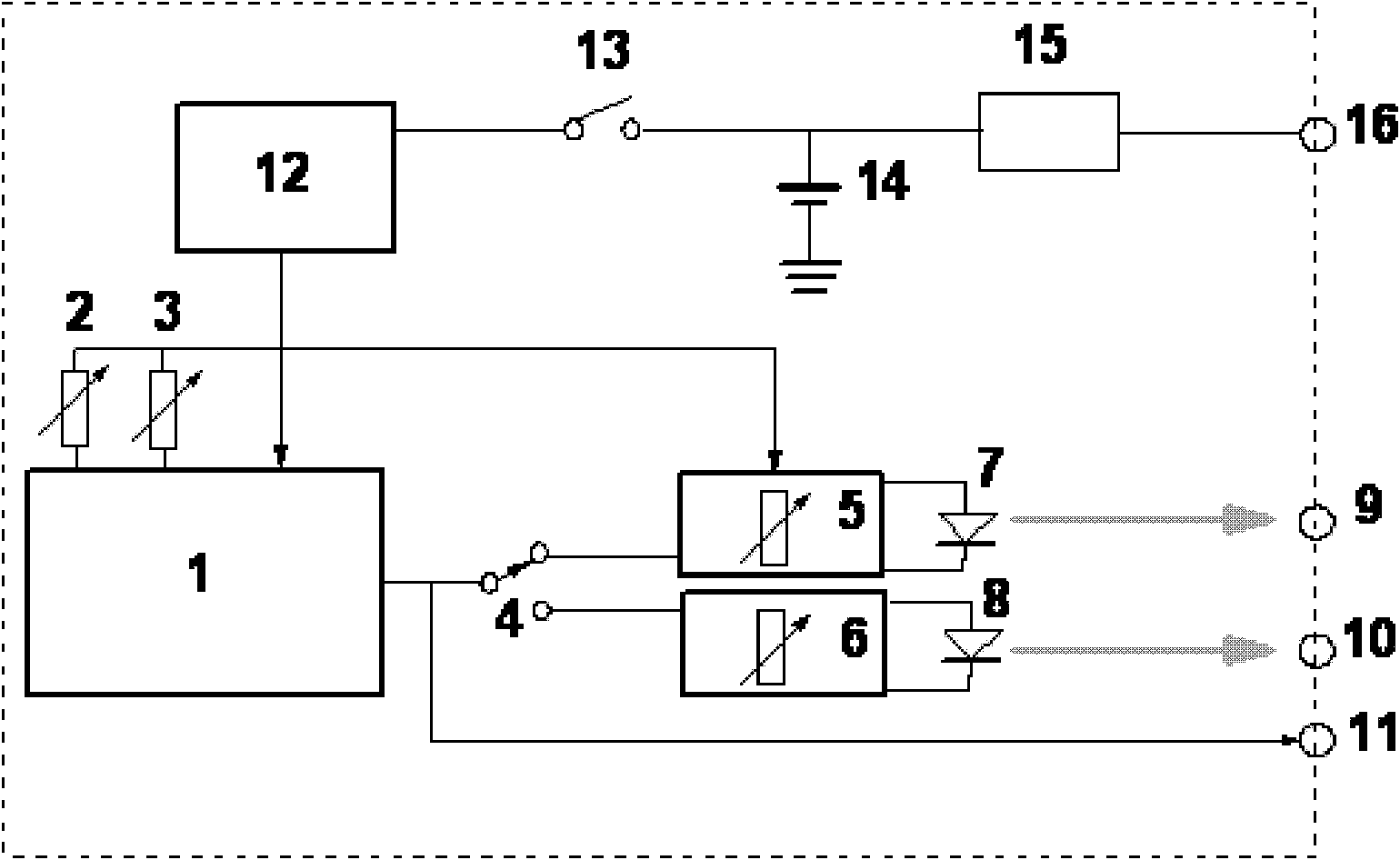
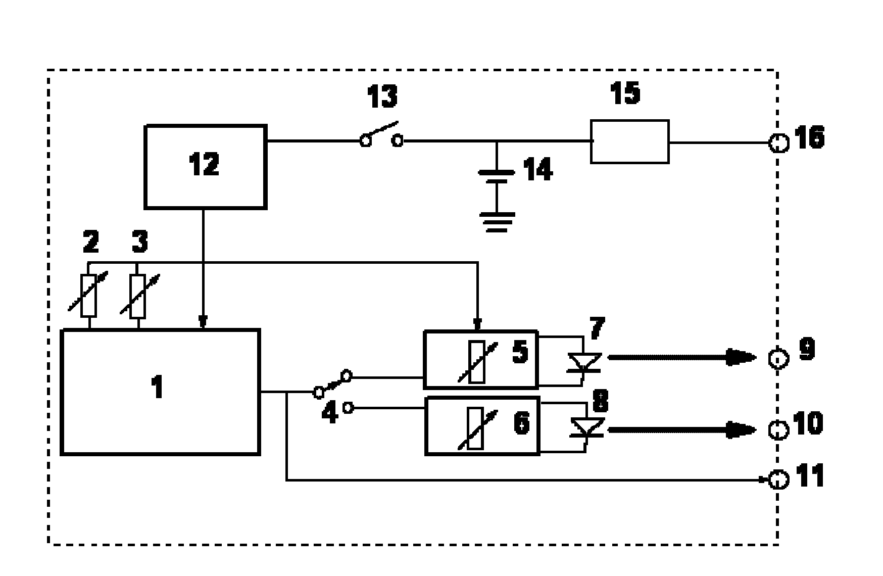
[0011] Below in conjunction with specific embodiment, further illustrate the present invention. It should be understood that these examples are only used to illustrate the present invention and are not intended to limit the scope of the present invention. In addition, it should be understood that after reading the content taught by the present invention, those skilled in the art may make various changes or modifications to the present invention, and these equivalent forms also fall within the scope defined by the appended claims of the present application.

[0012] like figure 1 As shown, the present invention includes a small-scale integrated circuit, a semiconductor light-emitting device and a switch-type drive circuit. The small-scale integrated circuit 1 is connected to two parallel adjustable resistors 2 and 3, a switch 4 and an electrical interface 11, respectively. The electrical interface 11 is used to monitor the pulse waveform and parameters, the two ends of the swi...


PUM


Abstract

The invention relates to a micro broad-pulse dual-wavelength optogenetic stimulation device which comprises a small-scale integrated circuit, semiconductor light-emitting devices and switch type driving circuits, wherein the small-scale integrated circuit is respectively connected with two adjustable resistors capable of independently adjusting pulse parameters within large ranges, a changeover switch and an electrical interface; the electrical interface is used for monitoring pulse waveforms and parameters; both ends of the changeover switch are respectively connected with the switch type driving circuits; the two switch type driving circuits are respectively connected with one semiconductor light-emitting device; light pulses of two wavelengths, which are sent out by the driven semiconductor light-emitting devices, are respectively coupled to a light output interface through an optical fiber to be output or are directly output by the optical fiber; and the small-scale integrated circuit is connected with a power supply through a micro voltage-stabilizing module. The invention is applicable to light-emitting diodes (LED) and laser diodes (LD), can be applied to laser diode-pumpedsolid or optical fiber lasers, has fine universality and generality, and can be implemented in a flexible mode.

Description

technical field [0001] The invention belongs to the technical fields of optoelectronics, microelectronics and gene optics, and in particular relates to a miniature wide-pulse dual-wavelength photosensitive gene stimulation device. Background technique [0002] The introduction of electrical stimulation in the fields of biology and medicine to produce specific effects or functions has a history of hundreds of years. It has become a means and technology widely used in these fields, and has already entered clinical medicine. The most typical application device is implantation. cardiac pacemaker. These battery-operated devices use tiny electronic circuits to generate specific electrical pulses that are fed into microelectrodes implanted in the body to produce the desired therapeutic function. In recent years, the so-called "brain pacemaker" used to treat Parkinson's disease and other types of brain neurological diseases has also begun to enter clinical application. Controllabi...

Claims


Application Information

Patent Timeline
Patent Type & Authority Applications(China)
IPC IPC(8): A61N5/06
Inventor 张永刚顾溢
Owner SHANGHAI INST OF MICROSYSTEM & INFORMATION TECH CHINESE ACAD OF SCI
Why Eureka
Try Eureka