Method for cleaning semiconductor silicon wafer

A technology for semiconductors and silicon wafers, applied in semiconductor/solid-state device manufacturing, electrical components, circuits, etc., can solve problems such as increased process complexity, achieve the effects of avoiding residues, simplifying process steps, and enhancing cleaning effects

Active Publication Date: 2011-08-17
SHANGHAI INTEGRATED CIRCUIT RES & DEV CENT
View PDF5 Cites 8 Cited by
  • Summary
  • Abstract
  • Description
  • Claims
  • Application Information

AI Technical Summary

Problems solved by technology

[0006] The object of the present invention is to provide a method for cleaning semiconductor silicon wafers, to solve the problem of increased process complexity caused by the existing cleaning solvent for cleaning photoresist

Method used


Image

  • Method for cleaning semiconductor silicon wafer
  • Method for cleaning semiconductor silicon wafer
  • Method for cleaning semiconductor silicon wafer

Examples


Embodiment Construction

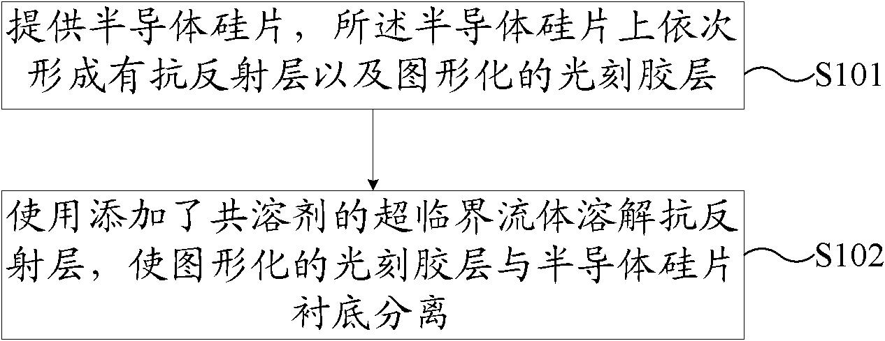
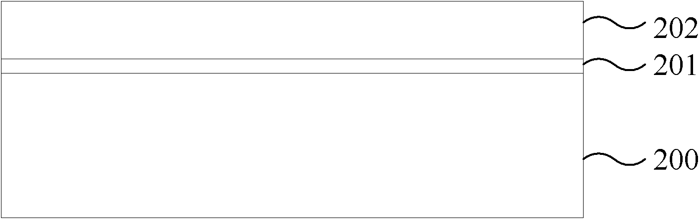
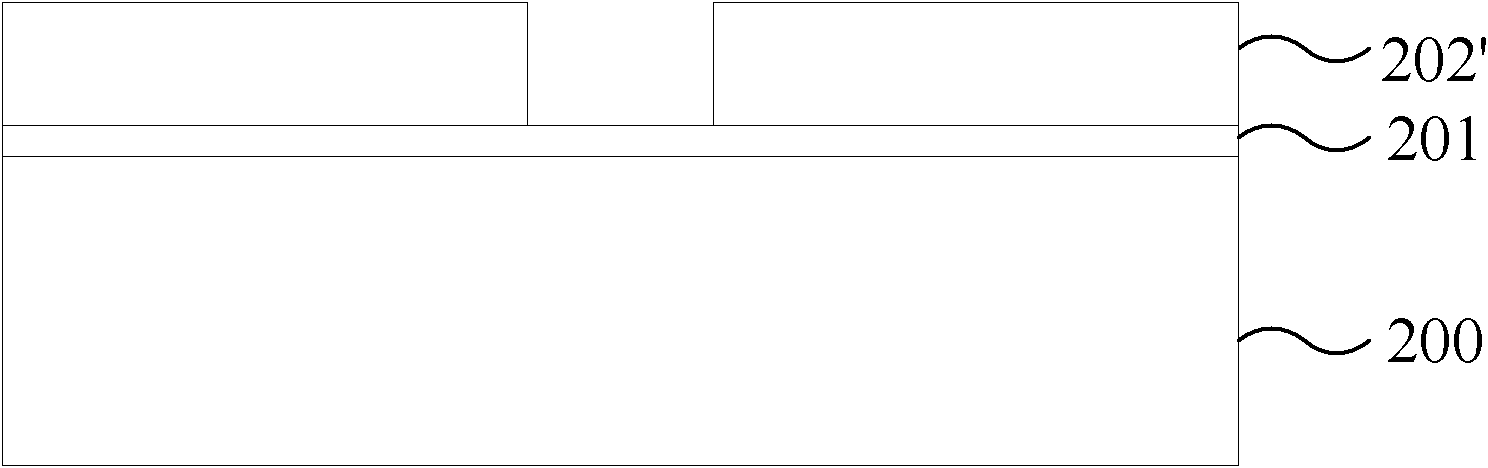
[0018] The method for cleaning semiconductor silicon wafers proposed by the present invention will be further described in detail below in conjunction with the accompanying drawings and specific embodiments. Advantages and features of the present invention will be apparent from the following description and claims. It should be noted that all the drawings are in very simplified form and use imprecise ratios, which are only used for the purpose of conveniently and clearly assisting in describing the embodiments of the present invention.

[0019] The core idea of ​​the present invention is to provide a method for cleaning semiconductor silicon wafers, which uses a supercritical fluid added with a co-solvent to dissolve the anti-reflection layer, so that the photoresist layer covered on the anti-reflection layer is Dissolving and detaching from the semiconductor silicon wafer, that is, the photoresist layer loses physical connection with the surface of the semiconductor silicon w...


PUM

PropertyMeasurementUnit
thicknessaaaaaaaaaa
thicknessaaaaaaaaaa

Abstract

The invention discloses a method for cleaning a semiconductor silicon wafer. The method comprises the following steps: providing the semiconductor silicon wafer, wherein an antireflecting layer and a graphical photoresist layer are formed on the semiconductor silicon wafer in sequence; and using supercritical fluid to which a cosolvent is added to dissolve the antireflecting layer so as to separate the graphical photoresist layer from the semiconductor silicon wafer. The method has the following beneficial effects: photoresist layer residues possibly caused by directly using a cleaning solvent to dissolve the photoresist layer are avoided, and adjustment of the components of the cleaning solvent according to different photoresist and processes is simultaneously avoided, thus greatly simplifying the cleaning process steps. In addition, the cleaning effect can be obviously improved by ensuring the photoresist layer to break away from the semiconductor silicon wafer by dissolving the antireflecting layer.

Description

technical field [0001] The invention relates to the technical field of integrated circuit technology, in particular to a method for cleaning semiconductor silicon wafers. Background technique [0002] With the continuous improvement of the integrated circuit manufacturing process, the volume of semiconductor devices is becoming smaller and smaller, so the material loss caused by the cleaning process is becoming more and more important. In state-of-the-art processes, the permissible material loss per wash is almost a very, very small amount, which is a considerable challenge for the cleaning process. Among them, due to the high-dose ion implantation process, a dehydrogenated and amorphous carbon layer will be formed on the surface of the photoresist. Therefore, the stripping of the photoresist layer after high-dose ion implantation is a severe problem. test. [0003] At present, the stripping process widely used in the industry is to ash the photoresist with oxygen plasma f...

Claims


Application Information

Patent Timeline
Patent Type & Authority Applications(China)
IPC IPC(8): H01L21/02G03F7/42
Inventor 张晨骋
Owner SHANGHAI INTEGRATED CIRCUIT RES & DEV CENT
Why Eureka
Try Eureka