
High-reliability capacitance type radio frequency micro-electromechanical system switch without charge injection effect

A charge injection effect, MEMS technology, applied in electrical switches, magnetic/electric field switches, circuits, etc., can solve problems such as reducing the amount of charge injection, low-frequency noise, and decreasing dielectric constant, and achieve improved reliability. Effect

Inactive Publication Date: 2013-04-03
SOUTHEAST UNIV
View PDF5 Cites 0 Cited by
  • Summary
  • Abstract
  • Description
  • Claims
  • Application Information

AI Technical Summary

Problems solved by technology

The existing methods to reduce the charge injection effect mainly include: (1) Select an insulating dielectric material with a low trap density such as PECVD silicon oxide. The disadvantage is that the dielectric constant of the material is correspondingly reduced, thereby reducing the capacitance ratio of the switch; ( 2) Using bipolar bias voltage and making the polarity change cycle shorter than the charge injection time of the dielectric layer reduces the amount of charge injection. The disadvantage is that the higher voltage waveform change frequency will generate a lot of low-frequency noise in the application system

Method used


Image

  • High-reliability capacitance type radio frequency micro-electromechanical system switch without charge injection effect
  • High-reliability capacitance type radio frequency micro-electromechanical system switch without charge injection effect

Examples


Embodiment

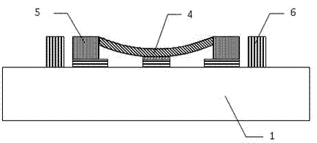
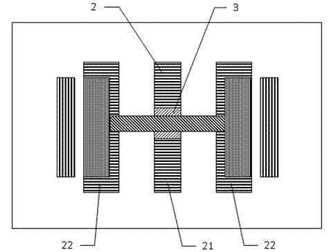
[0011] Example: like figure 1 , figure 2 As shown, the manufacturing process of the capacitive radio frequency MEMS switch of the present invention comprises the following steps:

[0012] (1) Sputter gold on a low-loss substrate and etch to form a coplanar waveguide;

[0013] (2) Deposit a layer of insulating dielectric film and etch only the part covering the overlapping area between the center electrode of the coplanar waveguide and the membrane bridge;

[0014] (3) Coating a sacrificial layer, and etching a movable bias electrode window on the sacrificial layer;

[0015] (4) Sputter gold and etch to form membrane bridges and movable bias electrode patterns, and then perform soft gold electroplating to thicken to form membrane bridges and movable bias electrode structures;

[0016] (5) Coat the sacrificial layer again, cover the film bridge and the movable bias electrode, and etch the fixed bias electrode window on the sacrificial layer;

[0017] (6) Sputter gold and...


PUM


Abstract

The invention relates to a high-reliability capacitance type radio frequency micro-electromechanical system switch without charge injection effect. A coplanar waveguide used as a radio frequency transmission line is produced on a low-loss substrate, a layer of insulating medium thin film covers the middle part of a central electrode of the coplanar waveguide, a switch film bridge spans over the insulating medium thin film, movable bias electrodes which are produced on a ground electrode of the coplanar waveguide are arranged at two ends of the film bridge, fixed bias electrodes are arranged at the outer sides of the movable bias electrodes, and the film bridge and the movable bias electrodes are both made of flexible electroplated gold. By adopting the flexible gold film bridge, the film bridge droops naturally and contacts the insulating medium thin film on the central electrode of the coplanar waveguide to realize the close state of the switch; furthermore, by applying lateral bias voltage between the movable bias electrodes and the fixed bias electrodes, the flexible gold movable bias electrodes can deviate outwards, the film bridge is tensioned so that the middle drooping partof the film bridge is separated from the insulating medium thin film and deviates upwards for a certain height to realize the open state of the switch. Therefore, the charge injection effect generated by the longitudinal bias voltage applied for realizing and maintaining the close state of the switch can be avoided, and the reliability of the switch can be improved.

Description

technical field [0001] The invention relates to a new capacitive radio frequency micro-electromechanical system switch. Background technique [0002] The charge injection effect of capacitive RF MEMS switches is considered to be the main cause of switch failure. The existing methods to reduce the charge injection effect mainly include: (1) Select an insulating dielectric material with a low trap density such as PECVD silicon oxide. The disadvantage is that the dielectric constant of the material is correspondingly reduced, thereby reducing the capacitance ratio of the switch; ( 2) Using a bipolar bias voltage and making the polarity change cycle shorter than the charge injection time of the dielectric layer reduces the amount of charge injection. The disadvantage is that the higher voltage waveform change frequency will generate a lot of low-frequency noise in the application system. Contents of the invention [0003] Technical problem: The purpose of the present inventio...

Claims


Application Information

Patent Timeline
Patent Type & Authority Patents(China)
IPC IPC(8): H01H36/00
Inventor 赵成黄庆安
Owner SOUTHEAST UNIV
Learn More