Method for doubly setting and accurately positioning centre of silicon slice

A precise positioning, silicon chip technology, applied in the direction of measuring devices, instruments, electrical components, etc., can solve the problems of strict camera environment requirements, excessive focus distance, etc., to save transmission time, eliminate secondary errors, simple and high-speed setting method Effect

Active Publication Date: 2011-08-31
SHENYANG KINGSEMI CO LTD
View PDF4 Cites 21 Cited by
  • Summary
  • Abstract
  • Description
  • Claims
  • Application Information

AI Technical Summary

Problems solved by technology

[0006] The purpose of the present invention is to provide a double-setting method for accurately identifying and relocating the center of the silicon wafer, so as to solve the problems in the prior art that the focusing distance required for scanning the edge of the silicon wafer is too large, and the imaging environment is strict. The position error generated during the silicon wafer transmission process, the method of repositioning before the silicon wafer process

Method used


Image

  • Method for doubly setting and accurately positioning centre of silicon slice
  • Method for doubly setting and accurately positioning centre of silicon slice
  • Method for doubly setting and accurately positioning centre of silicon slice

Examples


Embodiment 1

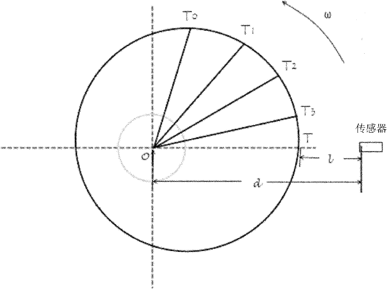
[0050] Embodiment 1, set the diameter of the silicon wafer to be 2 inches

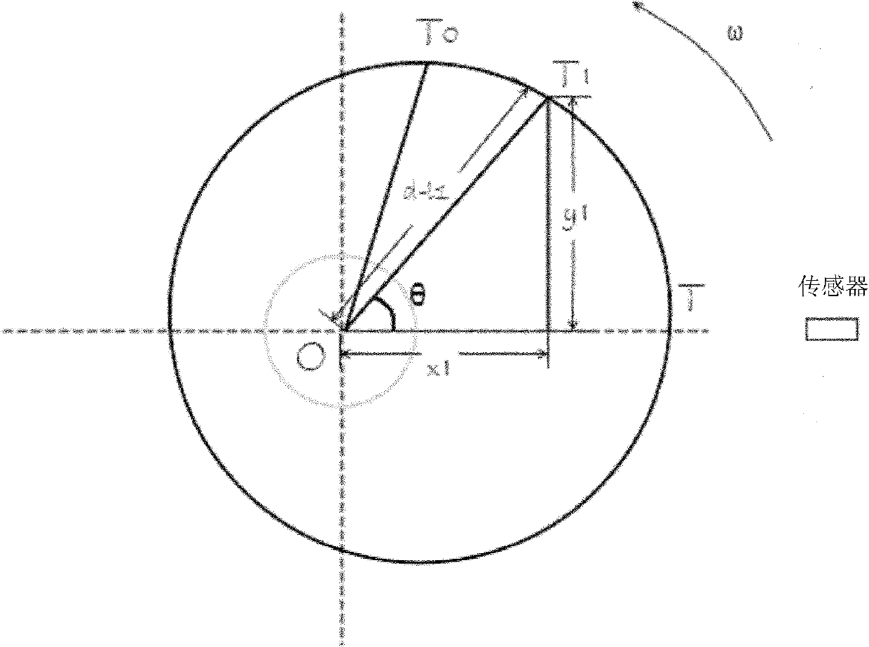
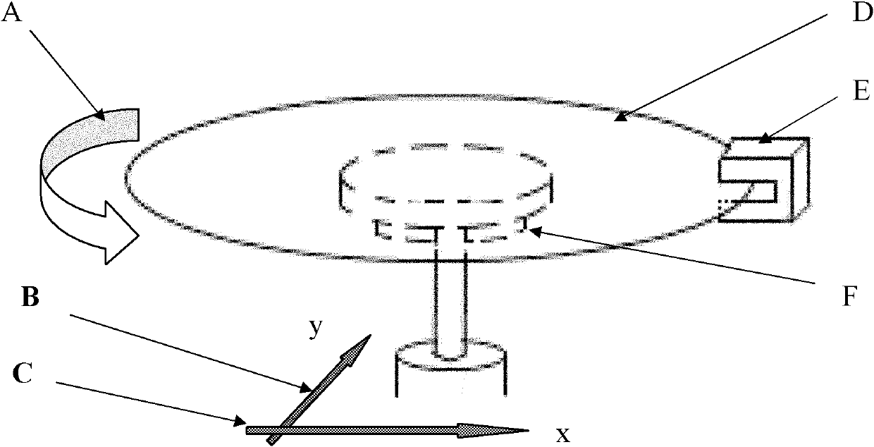
[0051] First, place the processing carrier silicon wafer D on the wafer stage; then rotate the silicon wafer D counterclockwise with a rotation angle of 30°, and at the same time, the edge of the silicon wafer is detected by a low-precision linear image recognition sensor installed on the side of the edge of the silicon wafer. Detection; the detection value is calculated by the formulas (1), (2), (3), and (4), and the position of the flat edge or notch of the silicon wafer and the position of the circle center are located; in the first time, the distance d from the sensor to the center O of the wafer stage =35mm, the angular velocity of the silicon wafer rotation is ω=0.1047 radian / second; the moment t when the timing starts 0 is: 0s, timing time t 1 For: 1s, t 2 is: 2s, t 3 is: 3s, the time t to stop timing is: 5s; time t 1 , time t 2 , time t 3 , the distance from the corresponding sensor to th...


PUM


Abstract

The invention relates to a processing technology of a silicon slice for manufacturing of an integrated circuit, in particular to a method for doubly setting and accurately positioning the centre of the silicon slice. The method comprises the following steps of: rotating the silicon slice along centre direction; identifying edges of the silicon slice sequentially by linear image identification sensors having different precisions; determining positions of a flat edge or a notch; determining the offset of the centre of the silicon slice; and moving the silicon slice by using a bidirectional movement motor to make the centre of the silicon slice overlapped with a designed position. Therefore, a transmission error of the silicon slice existing in processing equipment in the process of semiconductor industry is avoided, and the precision of the set centre of the silicon slice is equal to 1 mu m by using the double-setting method.

Description

technical field [0001] The invention relates to a silicon chip processing technology for integrated circuit manufacturing, in particular to a double-setting method for precisely locating the center of a silicon chip. Background technique [0002] Automatic equipment in the semiconductor field will inevitably produce transmission errors during the transmission of silicon wafers. These errors are manifested as the center of the silicon wafer is offset. In order to avoid the process defects caused by the offset, the silicon wafer needs to be repositioned before the process is processed. [0003] The mechanical clamping method used in the original semiconductor automatic equipment repositions the silicon wafer. This method requires a specific structure to contact the silicon wafer to reposition it. When the specific structure leaves the silicon wafer, it may cause secondary errors. In order to reduce the secondary error, the mechanical clamping method improves the contact surfa...

Claims


Application Information

Patent Timeline
Patent Type & Authority Applications(China)
IPC IPC(8): H01L21/02H01L21/66G01B11/00
Inventor 郑春海康宁田广霖
Owner SHENYANG KINGSEMI CO LTD
Why Eureka
Try Eureka