Method of manufacture of a multi-layer phosphorescent organic light emitting device, and articles thereof

A device, phosphorescence technology, applied in the field of manufacturing multilayer phosphorescent organic light-emitting devices

Inactive Publication Date: 2011-08-31
GENERAL ELECTRIC CO
View PDF2 Cites 10 Cited by
  • Summary
  • Abstract
  • Description
  • Claims
  • Application Information

AI Technical Summary

Problems solved by technology

The biggest challenge is related to the solubility of phosphorescent materials in most organic solvents

Method used


Image

  • Method of manufacture of a multi-layer phosphorescent organic light emitting device, and articles thereof
  • Method of manufacture of a multi-layer phosphorescent organic light emitting device, and articles thereof
  • Method of manufacture of a multi-layer phosphorescent organic light emitting device, and articles thereof

Examples


Embodiment

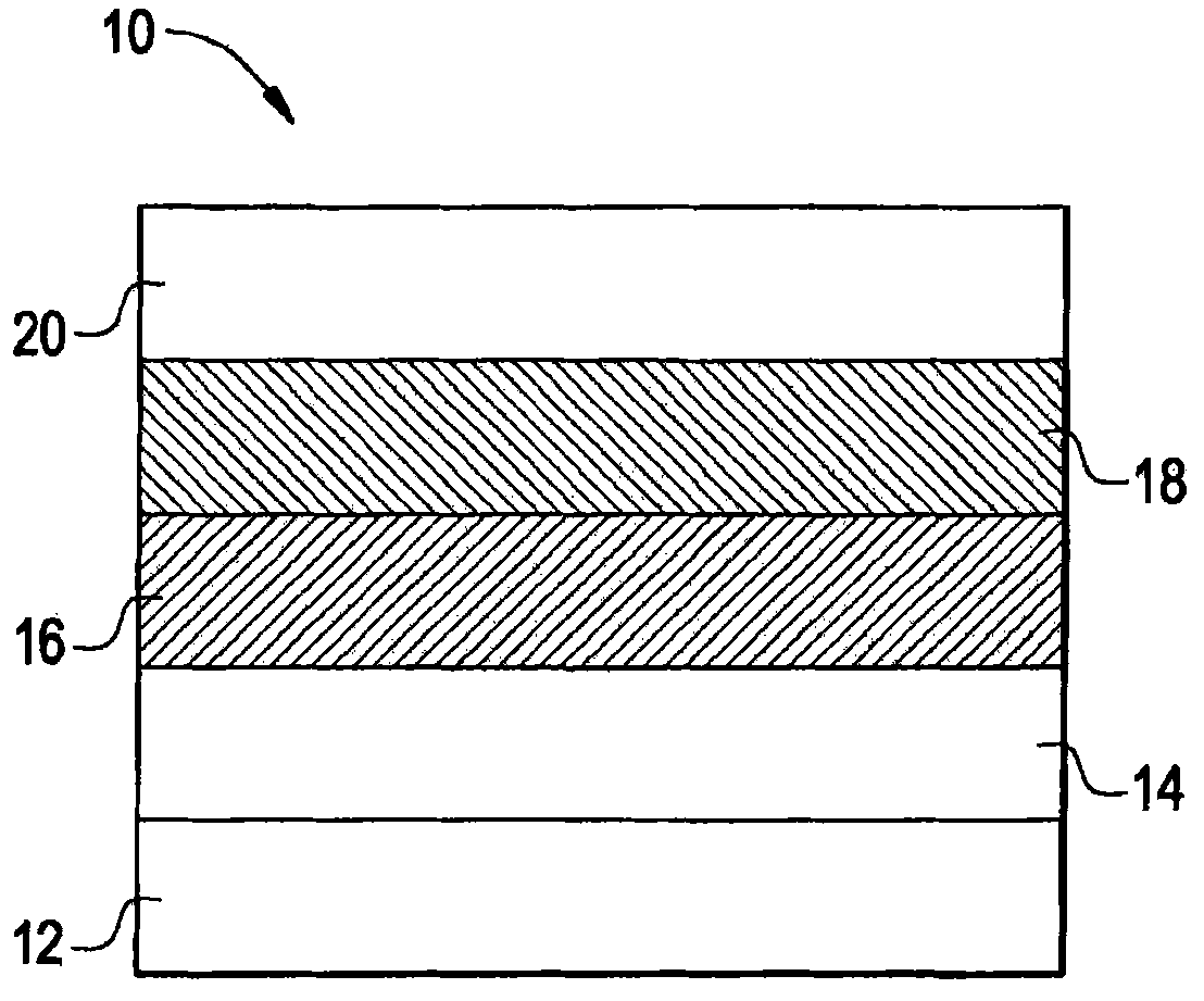
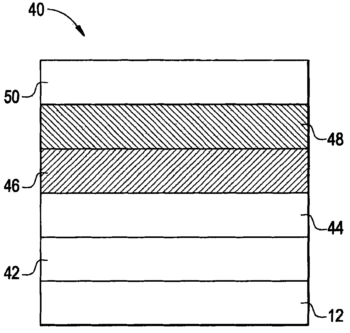
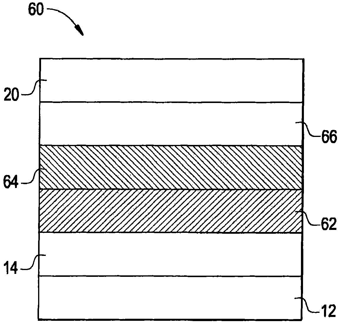
[0105] The multilayer phosphorescent OLED was constructed as follows. A phosphorescent OLED includes a blue phosphorescent polymer light-emitting layer and a red phosphorescent layer. Pre-patterned ITO-coated glass was used as the anode substrate and cleaned with UV-ozone for 10 minutes. A layer (60 nm) of polystyrenesulfonic acid-doped poly(3,4-ethylenedioxythiophene) (PEDOT:PSS) obtained from H.C. Starck was deposited on top of ITO by spin coating, followed by air Bake at 180°C for 1 hour. The coated substrate was then transferred into an argon-filled glove box (humidity and oxygen less than 1 ppm). A blue phosphorescent polymer emitting layer of 275-44-5 (about 30 nm thick) was subsequently spin-coated on top of the PEDOT:PSS layer from a chlorobenzene solution and baked on a hotplate (preheated to 120 °C) 10 minutes. Next, OXD-7 (1,3-bis[(p-tert-butyl)phenyl-1,3,4- A mixture of oxadiazolyl]benzene) and ADS069RE in a weight ratio of 90:10 (OXD-7:ADS069RE) was spin-cas...


PUM

PropertyMeasurementUnit
thicknessaaaaaaaaaa

Abstract

A method for forming multi-emissive phosphorescent layers for a phosphorescent OLED comprises coating a first phosphorescent material from a first solvent onto a first electrode and removing the first solvent to form a first emissive layer; and coating a second phosphorescent material from a second solvent onto the first emissive layer and removing the second solvent to form a second emissive layer, wherein the first and second emissive layers are not cured after coating, and wherein the first emissive layer has negligible solubility in the second solvent.

Description

Background of the invention [0001] In general, the present invention relates to methods of making multilayer phosphorescent organic light emitting devices and articles thereof. [0002] An organic light emitting device (OLED) having a multilayer structure is generally preferred to achieve high performance and meet specific requirements such as white light required for lighting. Phosphorescent materials are desired in OLEDs because they can efficiently achieve 100% internal quantum efficiency (IQE), compared to 25% for fluorescent materials. [0003] Current state of the art phosphorescent materials in the form of small molecules can be utilized. Small-molecule-based multilayer phosphorescent OLEDs are usually fabricated by vacuum-depositing organic materials, which suffers from high cost and low throughput. [0004] Multilayer phosphorescent OLEDs fabricated by solvent coating such as gravure coating, screen printing, and other solvent coating methods are not described, alth...

Claims


Application Information

Patent Timeline
Patent Type & Authority Applications(China)
IPC IPC(8): H01L51/50H01L51/00
CPCH01L51/0007H01L51/0043H01L51/0037C08G2261/512H01L51/5036C08G2261/3223H01L51/0085H01L51/0072H01L2251/5361C08G2261/1424H01L51/004H01L51/5016H10K71/15H10K85/1135H10K85/141H10K85/151H10K85/342H10K85/6572H10K50/125H10K50/11H10K2101/10Y10S428/917
Inventor 刘杰K·S·奇查克A·R·杜加尔叶青
Owner GENERAL ELECTRIC CO
Why Eureka
Try Eureka