Non-conducting decoration film

A decorative film and thin-layer technology, applied in the field of non-conductive decorative film, can solve problems such as inaccurate control of indium film thickness and uniformity, high cost, and impact on non-conductivity, etc., to achieve huge market potential and market value, non-conductivity High and strong adhesion effect

Inactive Publication Date: 2011-09-07
东莞市东日光学科技有限公司
View PDF6 Cites 0 Cited by
  • Summary
  • Abstract
  • Description
  • Claims
  • Application Information

AI Technical Summary

Problems solved by technology

Since indium is a rare metal, it has a high cost and cannot be popularized and promoted; the color is relatively single and can only present a certain color effect; the process is complicated, and the thickness and uniformity of the indium film cannot be accurately controlled. The uneven thickness of the indium film will directly affect the non-conductive effect; the electromagnetic radiation generated by the mobile phone cannot be completely shielded; it can only be attached to the surface of glass products, etc.
[0004] Therefore, the prior art can no longer meet the requirements of society and consumers for decorative films.

Method used


Image

  • Non-conducting decoration film
  • Non-conducting decoration film
  • Non-conducting decoration film

Examples


Embodiment 1

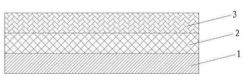
[0013] Example 1, see figure 1 , a non-conductive decorative film of the present invention, the number of thin layers of the non-conductive decorative film is 3 layers, from top to bottom are respectively the first thin layer 1 of silicon oxide, the second thin layer 2 of titanium oxide, and the second thin layer of titanium oxide. Three thin layers3.

Embodiment 2

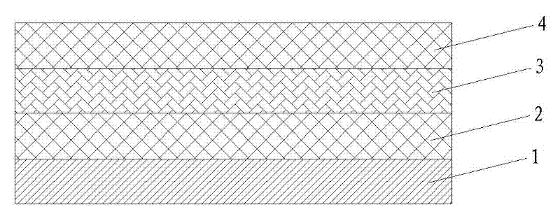
[0014] Example 2, see figure 2 , a non-conductive decorative film of the present invention, the number of thin layers of the non-conductive decorative film is 4 layers, from top to bottom are respectively the first thin layer 1 of silicon oxide, the second thin layer 2 of titanium oxide, and the second thin layer of titanium oxide. Three thin layers 3, a fourth thin layer 4 of titanium oxide.

Embodiment 3

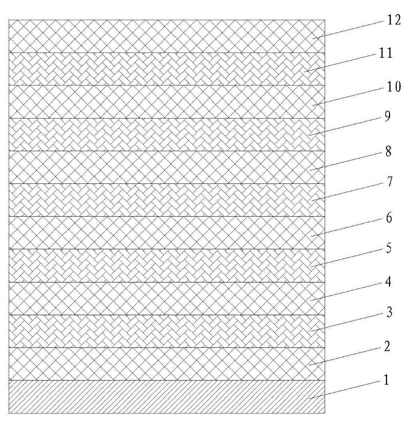
[0015] Embodiment 3, see image 3 , a non-conductive decorative film of the present invention, the number of thin layers of the non-conductive decorative film is 12 layers, from top to bottom are respectively the first thin layer 1 of silicon oxide, the second thin layer 2 of titanium oxide, and the second thin layer of titanium oxide. Three thin layers 3, fourth thin layer 4 of titanium oxide, fifth thin layer 5 of titanium oxide, sixth thin layer 6 of titanium oxide, seventh thin layer 7 of titanium oxide, eighth thin layer 8 of titanium oxide, ninth thin layer of oxide Layer 9, a tenth thin layer 10 of titanium oxide, an eleventh thin layer 11 of titanium oxide, and a twelfth thin layer 12 of titanium oxide.


PUM


Abstract

The invention discloses a non-conducting decoration film which comprises a first silicon oxide thin layer, second titanium oxide thin layers and third zirconium oxide thin layers, wherein the second titanium oxide thin layers and the third zirconium oxide thin layers are formed from the lower surface of the first silicon oxide thin layer from top to bottom; the non-conducting decoration film has 3-12 thin layers; and the second to twelfth thin layers are formed in such a way that the titanium oxide thin layers and the zirconium oxide thin layers are arranged alternately. The non-conducting decoration film provided by the invention has reasonable design and novel conception, can be widely applied to various electronic products and living products, and has huge market potential and market value.

Description

technical field [0001] The invention relates to the technical field of decorative films, in particular to a non-conductive decorative film. Background technique [0002] Decorative films are widely used in various electronic products such as mobile phones, electronic game consoles, etc., as well as various lighting, jewelry boxes, decorations, etc., to improve their decorative and visual effects. [0003] The traditional decorative film is generally coated with a layer of indium film on the surface of the product. Since indium is a rare metal, it has a high cost and cannot be popularized and promoted; the color is relatively single and can only present a certain color effect; the process is complicated, and the thickness and uniformity of the indium film cannot be accurately controlled. The uneven thickness of indium film will directly affect the non-conductive effect; it cannot completely shield the electromagnetic radiation generated by mobile phones; it can only adhere t...

Claims


Application Information

Patent Timeline
Patent Type & Authority Applications(China)
IPC IPC(8): B32B9/04
Inventor 陈沛洪
Owner 东莞市东日光学科技有限公司
Why Eureka
Try Eureka