Vertical foldaway memory array structure
A memory array, foldable technology, applied in the field of vertical foldable flash memory array structure, can solve the problems of SONOS flash memory technology and complex control methods, etc., achieve high-density and large-capacity storage capacity, simple structure, and simplified production The effect of the manufacturing process
- Summary
- Abstract
- Description
- Claims
- Application Information
AI Technical Summary
Problems solved by technology
Method used
Image
Examples
Embodiment 1
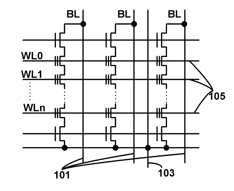
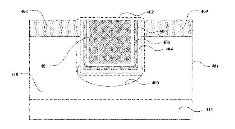
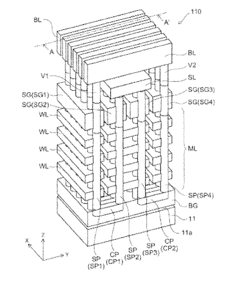
[0042] In an embodiment of the present invention, the proposed vertically foldable memory array structure includes: vertically foldable memory modules distributed in columns and rows, the vertically foldable memory modules include drain selection transistors, bottom connection lines and source selection transistors, and A plurality of memory cell transistors connected between the drain selection transistor and the bottom connection line and between the source selection transistor and the bottom connection line, wherein the gate structure of each memory cell transistor is connected to the A word line is connected, the drain of each said drain selection transistor is connected to a bit line, and the drain of the drain selection transistor in the Mth vertical folding memory module in the Nth column is connected to the Mth of the N+1th column -The sources of the source selection transistors in one vertically foldable memory module are all connected to the same bit line, and the gat...
Embodiment 2
[0060] The vertically folded memory structure according to Embodiment 2 of the present invention includes: memory cell transistor groups distributed in columns and rows, the memory cell transistor group includes a plurality of memory cell transistors, wherein each of the memory cell transistors has a gate structure Connected to a word line; a plurality of drain selection transistors and a plurality of source selection transistors, wherein each of the memory cell transistor groups in the Nth column is connected to a drain selection transistor, and the memory cell transistor group in the N+1th column Each of them is connected to a source selection transistor; a plurality of bottom selection transistors, and the bottom selection line connects the memory cell transistor group in the Mth row of the Nth column and the M+1th row of the N+1th column Between the memory cell transistor groups of the rows, wherein, the drains of the drain selection transistors and the source electrodes of...
PUM
 Abstract
Description
Claims
Application Information


