Groove type power MOSFET (Metal-Oxide-Semiconductor Field Effect Transistor) device

A device and power technology, applied in the field of semiconductor power devices and radio frequency power devices, can solve problems such as the inability to completely eliminate capacitance, and achieve the effects of eliminating epitaxial line inductance, reducing gate charge, and increasing carrier concentration

Inactive Publication Date: 2013-07-17
UNIV OF ELECTRONICS SCI & TECH OF CHINA
View PDF8 Cites 0 Cited by
  • Summary
  • Abstract
  • Description
  • Claims
  • Application Information

AI Technical Summary

Problems solved by technology

However, this structure still cannot completely eliminate the capacitance formed between the bottom of the trench gate and the drift region.

Method used


Image

  • Groove type power MOSFET (Metal-Oxide-Semiconductor Field Effect Transistor) device
  • Groove type power MOSFET (Metal-Oxide-Semiconductor Field Effect Transistor) device
  • Groove type power MOSFET (Metal-Oxide-Semiconductor Field Effect Transistor) device

Examples


Embodiment 1

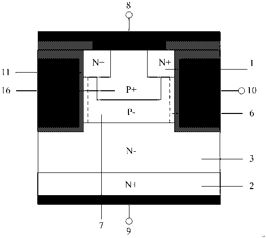
[0044] Taking N-channel devices as an example, the present invention is as Figure 4 shown, including N + Source area 1, N + Drain region 2, lightly doped drain region 3, N + Slot 4, N + Source contact region 5, channel region 6, P well region 7, source electrode 8, drain electrode 9, gate electrode 10, gate oxide 11, field oxide 12, surface source metal field plate 13, isolation oxide 14, P - Substrate 15.

[0045] Preferably, the thickness of the field oxide 12 should be controlled between 100nm~500nm. The thicker the field oxide, the weaker the effect of the source metal field plate, and the less obvious the effect of assisting the depletion of the lightly doped drain region. The field oxide should not be too thin to prevent parasitic channels on the silicon surface.

[0046] The slot-type power MOSFET devices mentioned above can also not be made of N + source region 1, its N + Groove area 4 is directly used as groove type N + Source region 4, forming a power MOSF...

Embodiment 2

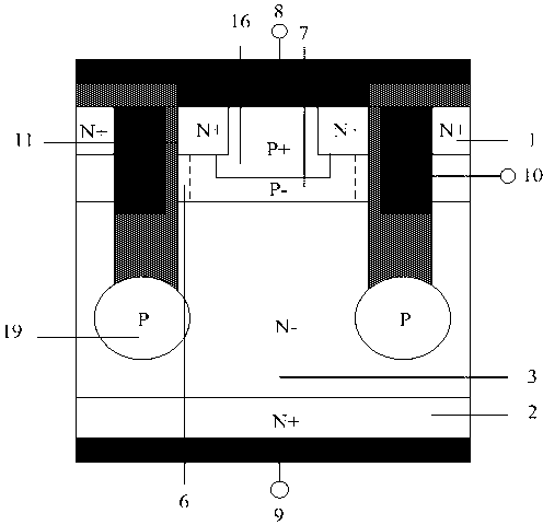
[0071] Figure 4~Figure 7 as well as Figure 12 , Figure 13 The grooved power MOSFET device, its N channel can also be made into a P channel, forming a P channel grooved power MOSFET device, and the device structure is as follows Figure 14 shown. The conductivity type of all semiconductor regions of a P-channel trench power MOSFET device should be opposite to that of an N-channel trench power MOSFET device.

Embodiment 3

[0073] The manufacturing process of the present invention is similar to the conventional LDMOS manufacturing process, and the following points need to be noted:

[0074] 1.P + The approach in the contact area: doing a good job in P - well contact area P + 1 Finally, a gap must be left for the next step of high-concentration P + injection to form P + 2 area, the surface metal covering will be P + 2 area and N + The source region is connected thus ensuring that the P - well area and N + The source region is equipotential. The device cross-section of this embodiment is shown in Figure 10(a), and the device layout is shown in Figure 10(c), where no surface metal coverage is shown. If P + 2 If the region adopts the scheme shown in Figure 10(b), it needs to be formed by ion implantation on the back side, and a gap needs to be left when making the source contact area on the back side, and the position of the gap is still the same as that shown in Figure 10(c).

[0075] ...


PUM


Abstract

The invention discloses a groove type power MOSFET (Metal-Oxide-Semiconductor Field Effect Transistor) device relating to the technical field of semiconductor power devices and radio frequency power devices. A surface N+ source region, a source metal field board and a bottom N+ source contact region are communicated to form an equipotential body in the mode that an N+ tank region passes through the substrate longitudinally to the bottom of the device; and the source is led out from the bottom of the device, so that the epitaxial line inductance of the source is eliminated, the series resistance of the source is reduced, and good heat conduction channels are provided for being beneficial to two-sided cooling of the device. Simultaneously, the source metal field board extended covers the light dope drain (LDD) so as to reduce the high electric field peak at the tail end of the grid and assist the light dope drain (LDD) to exhaust and reduce the grid leak capacitance. The charge balance effect of the light dope drain, the source metal field board and the P-substrate below improves the carrier concentration at the light dope drain and reduces the on resistance of the device to be minimum. The device reduces the gate charge under the premise of ensuring low on resistance, thus enabling the device to have lower power consumption and good heat dissipation characteristics.

Description

technical field [0001] The invention relates to the technical fields of semiconductor power devices and radio frequency power devices. Background technique [0002] Low-power MOSFETs play a very important role in switch-mode power systems. In the last two decades, slot VDMOS has become the most successful technology for low-voltage power switches. Its main advantage is that the high channel density results in a device with low on-resistance. However, the trench wall with a large area is not conducive to reducing the volume of the internal capacitance. With the improvement of integration, the switching speed of the device decreases and the power loss increases. In addition, the moderate doping of the epitaxial layer below the trench makes it impossible to adjust the impedance of the transistor. Existing trench VDMOS devices are usually made as figure 1 Structure shown, where 1 is N + source area, 2 is N + drain region, 3 is N - Drift region, 6 is the channel region, 7...

Claims


Application Information

Patent Timeline
Patent Type & Authority Patents(China)
IPC IPC(8): H01L29/06H01L29/78
Inventor 张波胡夏融罗小蓉李泽宏邓小川雷天飞姚国亮王元刚
Owner UNIV OF ELECTRONICS SCI & TECH OF CHINA
Why Eureka
Try Eureka