Digital pll circuit and communication apparatus

A circuit and digital technology, applied in the field of communication devices, can solve the problems of higher design difficulty, higher power consumption, and difficulty in reducing the area, and achieve the effect of good phase noise characteristics and low power consumption

Inactive Publication Date: 2011-09-14
PANASONIC CORP
View PDF4 Cites 2 Cited by
  • Summary
  • Abstract
  • Description
  • Claims
  • Application Information

AI Technical Summary

Problems solved by technology

[0015] However, the structure of the TDC312 requires an inverter chain long enough to cover one cycle of the output clock CKV in order to detect the rising / falling edges of the reference signal FREF and the output clock CKV, making it difficult to reduce the area.
In addition, if the frequency magnification factor FCW relative to the reference signal FREF is increased, the clock signal CKV input to the inverter chain 3121 will become high-speed, and the power consumption will increase.
In addition, since the outputs of the inverters need to be at equal intervals in time, equal-length wiring between the inverters is required, which causes problems such as increased design difficulty.

Method used


Image

  • Digital pll circuit and communication apparatus
  • Digital pll circuit and communication apparatus
  • Digital pll circuit and communication apparatus

Examples


Embodiment approach 1

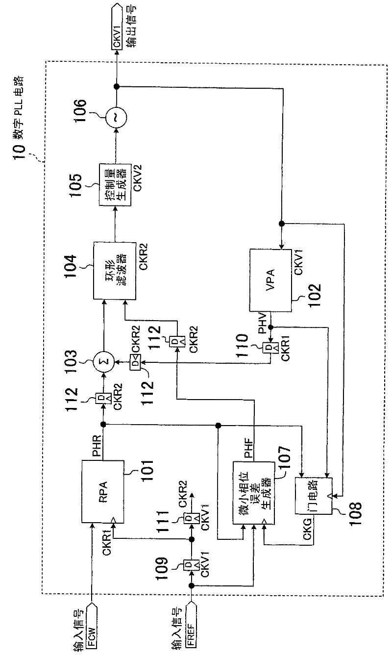
[0061] figure 1 The configuration of the digital PLL circuit according to the first embodiment of the present invention is shown.

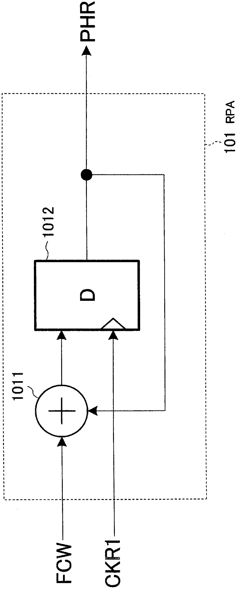
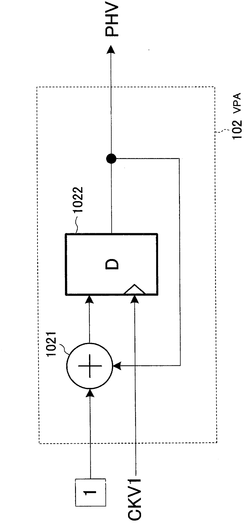
[0062] exist figure 1 Among them, 101 is the RPA circuit (Reference Phase Accumulator: reference phase calculator), 102 is the VPA circuit (Variable Phase Accumulator: variable phase calculator), 103 is the phase comparator (comparator), 104 is the phase error of the input 106 is a control oscillator, 105 is a control quantity generator that controls the control oscillator 106, 107 is a small phase error generator, and 108 is a small phase error generator. 109 is a gate circuit that generates a signal CKR1 that retimes the reference signal FREF in synchronization with the output clock CKV1, and 110 is a register circuit that operates in synchronization with the retiming signal CKR1. 111 is a register circuit that generates a signal CKR2 delayed by one clock from the retiming signal CKR1 , and 112 is a register circuit that operates in synchron...


PUM


Abstract

A digital PLL circuit for providing as an output a clock signal having a frequency obtained by multiplying the frequency of a reference signal by a frequency control word (frequency ratio). In the digital PLL circuit, an RPA circuit (101) sequentially adds frequency control words (FCW) each having a decimal component. An output from the RPA circuit (101) is supplied to a micro-phase-error generator (107), which generates, based on the decimal part of the sequentially added value of the frequency control words (FCW), a plurality of threshold values in the vicinity of the actual amplitude value of a reference signal (REF), and which then calculates, based on these threshold values, an amplitude value of the reference signal (REF) and also calculates a phase error of the reference signal (REF) in accordance with the calculated amplitude value, and which further calculates a micro-phase-error between the reference signal (REF) and an output clock (CKV1). Thus, even if the frequency control words include decimal components, the residual micro-phase-error between the reference signal and the output clock can be calculated and corrected in a smaller area and with a less power consumption.

Description

technical field [0001] The present invention relates to a digital PLL (Phase Locked Loop) circuit that outputs a clock signal of an arbitrary frequency in synchronization with a reference signal, and a communication device using the digital PLL circuit. Background technique [0002] Such as Figure 20 As shown, the existing general digital PLL circuit is composed of RPA circuit (Reference Phase Accumulator: reference phase calculator) 201 based on reference signal FREF work, VPA circuit (Variable Phase Accumulator: variable phase calculator) based on output clock CKV work ) 202, a phase comparator 203, a loop filter 204, and an oscillator 206. [0003] In the above-mentioned digital PLL circuit, the frequency of the output clock CKV is operated so that the frequency of the reference signal FREF is twice the frequency control word FCW (Frequency Command Word). For example, when the frequency of the reference signal FREF is 100MHz, if it is desired to obtain an output clock o...

Claims


Application Information

Patent Timeline
IPC IPC(8): H03L7/087H03L7/085
CPCH03L7/091H03L2207/50H03L7/087
Inventor 濑上史明冈本好史
Owner PANASONIC CORP
Why Eureka
Try Eureka