Method for determining highly accelerated stress screening test condition

A technology with high accelerated stress and test conditions, applied in electronic circuit testing, optics, measuring devices, etc., can solve the problems of reducing product competitiveness, restricting the production capacity of manufacturers, low efficiency, etc., to reduce product production cycle, reduce testing cost, and the effect of improving test efficiency

Inactive Publication Date: 2011-09-21
SHANGHAI MICRO ELECTRONICS EQUIP (GRP) CO LTD
View PDF2 Cites 17 Cited by
  • Summary
  • Abstract
  • Description
  • Claims
  • Application Information

AI Technical Summary

Problems solved by technology

[0005] First, the period required for product screening tests is long, generally 2-3 days;
[0006] Second, the work efficiency is low, which greatly restricts the production capacity of the manufacturer;
[0007] Third, it takes up a lot of equipment and high labor costs, resulting in excessively high production costs and reducing product competitiveness
[0008] With the rapid expansion of society's demand for electronic products, the production capacity of electronic companies is also expanding day by day. The shortcomings of long environmental screening test cycle, low efficiency and high cost seriously delay the time for electronic products to be introduced to the market, which restricts the development of electronic manufacturing companies.

Method used


Image

  • Method for determining highly accelerated stress screening test condition
  • Method for determining highly accelerated stress screening test condition

Examples


Embodiment 1

[0021] Example 1: Method for determining high-accelerated stress screening test conditions of hardware circuit boards

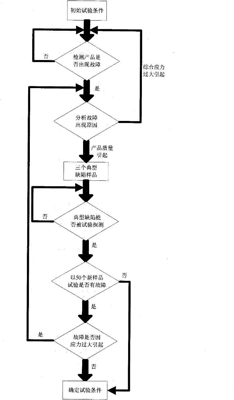
[0022] First, according to the highly accelerated life test of the hardware circuit board, the temperature operation limit of the temperature and vibration comprehensive stress of the hardware circuit board, the vibration damage limit and the rapid temperature change conduction operation limit are determined. Reduce the temperature operation limit of temperature and vibration comprehensive stress by 30%, reduce the vibration damage stress by 50%, take 80% of the rapid temperature conduction operation limit as the temperature change speed value, and keep the high and low temperature for 10 minutes as the initial test conditions. Temperature and vibration comprehensive stress test with sub-rapid temperature change cycle. On the basis of this initial test condition, gradually increase the initial stress by 15%, and perform more than one functional test during the t...

Embodiment 2

[0026] Embodiment 2: Method for determining high-accelerated stress screening test conditions of LCD module products

[0027] First, according to the high-accelerated life test of the LCD module, the temperature operation limit, the vibration damage limit and the rapid temperature change conduction operation limit of the LCD module's temperature and vibration comprehensive stress are determined. Reduce the temperature operation limit of the combined temperature and vibration stress by 30%, reduce the vibration damage stress by 50%, use 80% of the rapid temperature conduction operation limit as the temperature change speed value, and keep the high and low temperature for 15 minutes as the initial test conditions. Temperature and vibration comprehensive stress test with 6 rapid temperature change cycles. On the basis of the initial test conditions, gradually increase the initial stress by 10%, and perform more than one functional test during the temperature and vibration stabilizat...

Embodiment 3

[0031] Embodiment 3: Method for determining high-accelerated stress screening test conditions for semiconductor integrated circuit chip IC products

[0032] First, according to the highly accelerated life test of the semiconductor integrated circuit chip IC, the temperature operating limit of the temperature and vibration comprehensive stress of the semiconductor integrated circuit chip IC, the vibration damage limit and the rapid temperature change conduction operating limit are determined. Reduce the temperature operation limit of the combined temperature and vibration stress by 30%, reduce the vibration damage stress by 50%, use 80% of the rapid temperature conduction operation limit as the temperature change speed value, and keep the high and low temperature for 15 minutes as the initial test conditions. Temperature and vibration comprehensive stress test with 6 rapid temperature change cycles. On the basis of the initial test conditions, gradually increase the initial stress...


PUM


Abstract

The invention provides a method for determining a highly accelerated stress screening test condition. The method comprises the following steps of: firstly, setting an initial testing condition according to the temperature and vibration comprehensive stress operation and damage limit of a product to carry out temperature and vibration comprehensive stress test; accurately obtaining the highly accelerated stress screening test condition by using a successive approximation method; and then verifying by using a typical defect of the product to obtain the validity of the screening test condition; and finally, obtaining the effective highly accelerated stress screening test condition of the temperature and vibration comprehensive stress through repeated tests and scientific adjustment. By using the test condition obtained by using the method provided by the invention, the screening test time can be largely reduced, the testing efficiency can be increased and the test cost can be saved.

Description

Technical field [0001] The invention relates to a testing method of a hardware circuit board, in particular to a method for determining high-accelerated stress screening test conditions. Background technique [0002] With the widespread application of electronic products, people's requirements for the quality of electronic products are also increasing, and the life of electronic products has become an important criterion for product quality. However, in the product manufacturing process, due to material defects, out-of-control process, equipment instability and other related objective factors, it is inevitable that some electronic products have potential non-design defects when they leave the factory. Later potential defects will gradually be exposed and lead to rapid product failure, greatly shortening the product life. [0003] The distribution of failures after the product arrives on the market can be represented by the "bathtub curve" commonly used in industrial production. A...

Claims


Application Information

Patent Timeline
Patent Type & Authority Applications(China)
IPC IPC(8): G01R31/28G01R31/02G01R31/00G02F1/13
Inventor 朱辉李平池峰
Owner SHANGHAI MICRO ELECTRONICS EQUIP (GRP) CO LTD
Why Eureka
Try Eureka