Cathode patterns of electric semiconductor device and patterned arrangement method of cathode fingers thereof

A technology for power semiconductors and cathode strips, applied in semiconductor devices, electrical components, circuits, etc., can solve the problems of waste, reduce the utilization rate of chip area, large waste, etc., to improve uniformity, ensure convenience and practicability, The effect of improving gate characteristics

Active Publication Date: 2011-10-12
ZHUZHOU CRRC TIMES SEMICON CO LTD
View PDF0 Cites 4 Cited by
  • Summary
  • Abstract
  • Description
  • Claims
  • Application Information

AI Technical Summary

Problems solved by technology

However, each partition has a waste of irregular areas at the junction of rectangles and arcs, which reduces the utilization rate of the chip area, and the waste increases with the increase of the graphic radius, which is not suitable for large-diameter full-control devices
[0007] It can be seen from the above that the three comb arrangement methods have their own advantages and disadvantages, so the development of a cathode pattern of semiconductor devices with high chip area ratio, easy processing and molding, and suitable for various sizes and gate configurations become an urgent problem to be solved

Method used


Image

  • Cathode patterns of electric semiconductor device and patterned arrangement method of cathode fingers thereof
  • Cathode patterns of electric semiconductor device and patterned arrangement method of cathode fingers thereof
  • Cathode patterns of electric semiconductor device and patterned arrangement method of cathode fingers thereof

Examples


specific Embodiment approach

[0050] A specific embodiment of a method for arranging a cathode comb pattern of a power semiconductor device, comprising the following steps:

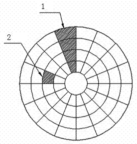
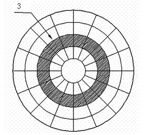
[0051] (A) Divide the cathode surface of the power semiconductor device into equal sectors with the center of the circle as the axis;

[0052] (B) Divide concentric rings on the cathode side of the power semiconductor device according to the length of the comb;

[0053] (C) Arrange combs in the sector, arrange the combs distributed in the sector and in the same ring along the circular arc of the ring, so that the outer edge of each circle of combs is a circular arc, and the combs The orientation of the bar setting is parallel to the center line of the sector;

[0054] (D) Reserve a gate shortcut channel between two adjacent sectors;

[0055] (E) The gate is provided in the central area or the ring area or the edge ring area of ​​the cathode face;

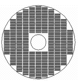
[0056] (F) Process the photolithographic mask designed according to the above steps ...


PUM


Abstract

The invention discloses cathode patterns of an electric semiconductor device and a patterned arrangement method of cathode fingers thereof, which are widely applied in the design of cathode patterns in an electric semiconductor, an electric electronic device, an all-controlled thyristor and the like. The cathode patterns comprises equant sector areas and concentric rings which are divided with a circle centre as an axle; the intersecting places of the sector areas and the concentric rings are pattern units; fingers distributed in the sector areas and located in one ring are arranged along a circle arc of the ring; the outer edge lines of each circle of fingers are circular arcs; and the directions of the fingers are all parallel to the centre lines of the sector areas; and gate pole fast channels are left between adjacent two sector areas. The cathode patterns are transferred to the surfaces of chips by photoetching the designed photomask plates to finish the final manufacturing. According to the cathode patterns and the patterned arrangement method of the cathode fingers thereof, the utilization rate of the effective areas of the chips is increased; the opening / closing uniformityof each finger is improved; the balancing of the opening / closing difference of the fingers, caused by the distance from gate pole electrodes is facilitated; and the machining formation is conveniently realized.

Description

technical field [0001] The invention relates to a power semiconductor device in the field of semiconductor devices and a design method thereof, in particular to a cathode pattern and a method for arranging the cathode comb pattern applied to power semiconductors, power electronic devices, fully-controlled thyristors, and the like. Background technique [0002] Cathode pattern design is the basic link in the design of various electronic devices, especially for fully controlled thyristors. The cathode pattern of the fully-controlled thyristor is complementary to the gate pattern, and directly affects the dynamic parameters of the device, so the graphic design of the fully-controlled thyristor must be cautious. Generally, after balancing the various parameters of the device, a rough graphic is designed, and the final graphic is determined by combining the designer's aesthetic style and the graphic characteristics of the company. The designed pattern is then transferred to the ...

Claims


Application Information

Patent Timeline
Patent Type & Authority Applications(China)
IPC IPC(8): H01L29/41H01L21/28
Inventor 陈芳林程银华陈勇民彭文华张明
Owner ZHUZHOU CRRC TIMES SEMICON CO LTD
Why Eureka
Try Eureka