Delay signal generating circuit
A technology for generating circuits and delaying signals, applied in the field of signal delay, can solve problems such as high circuit power consumption, and achieve the effect of reducing dynamic power consumption
- Summary
- Abstract
- Description
- Claims
- Application Information
AI Technical Summary
Problems solved by technology
Method used
Image

Examples
Embodiment Construction
[0017] In order to make the object, technical solution and advantages of the present invention clearer, the present invention will be further described in detail below in conjunction with the accompanying drawings and embodiments. It should be understood that the specific embodiments described here are only used to explain the present invention, not to limit the present invention.
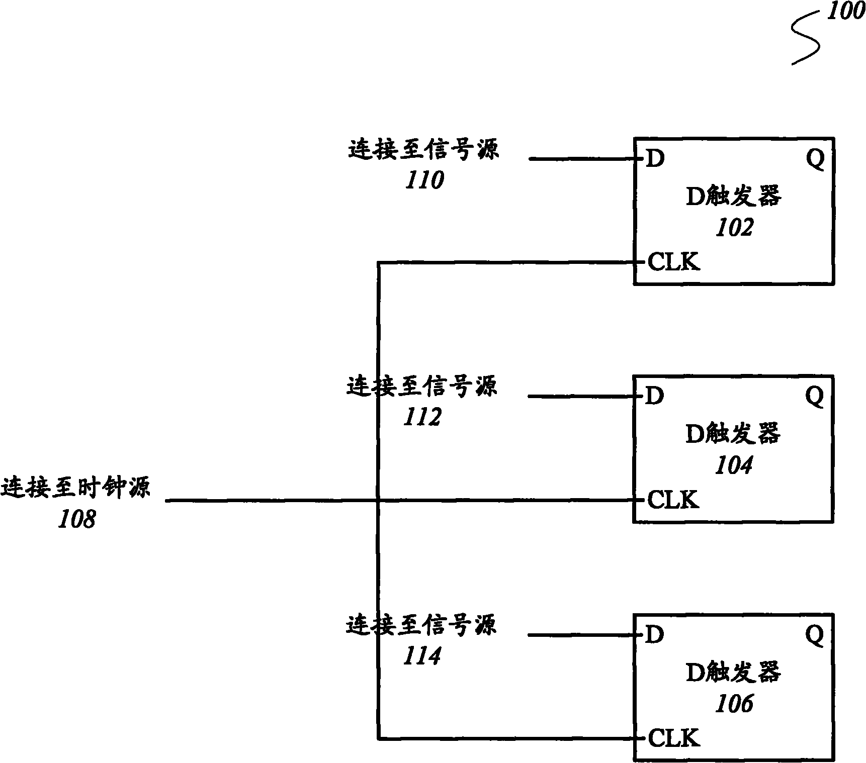
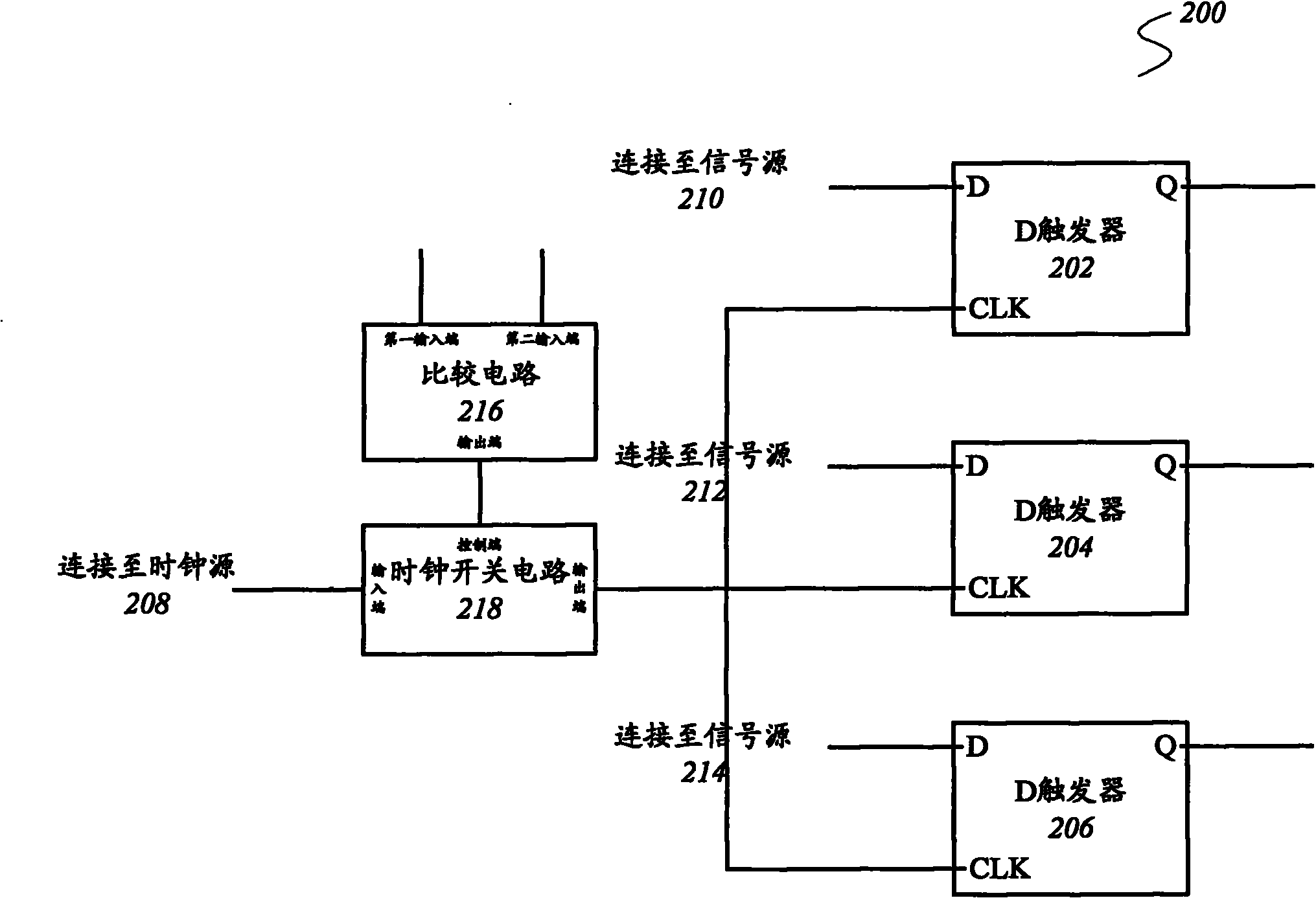
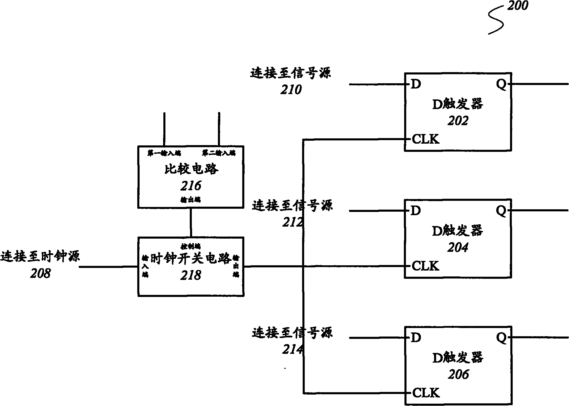
[0018] The invention provides a delayed signal generating circuit, which can output an invalid clock signal to a D flip-flop when the delayed signal is the same as the signal to be delayed. In this case, the D flip-flop will not sample the data signal from the source, thus greatly reducing dynamic power consumption. The delay signal generation circuit provided by the present invention will be described in detail below.
[0019] figure 2 is a circuit diagram of a delay signal generating circuit 200 according to a preferred embodiment of the present invention. Such as figure 2 As shown, the del...
PUM
 Abstract
Description
Claims
Application Information