Apparatus for automatically inspecting defects of PCB (printed circuit board)

A PCB circuit board, automatic inspection technology, applied in the direction of measuring devices, material analysis through optical means, instruments, etc., can solve the problems of high mechanical movement precision, high maintenance technical requirements, low manufacturing cost, etc., and achieve a high degree of automation , high detection accuracy and low manufacturing cost

Inactive Publication Date: 2011-10-19
MEIZHOU TAIYUAN TECH
View PDF5 Cites 30 Cited by
  • Summary
  • Abstract
  • Description
  • Claims
  • Application Information

AI Technical Summary

Problems solved by technology

However, the operator needs to put the PCB circuit board to be inspected on the inspection table, and manually mark the detected defect position, then manually take it out and enter the next repair process
This kind of mechanical inspection relies on manual operation, the degree of automation is low, the inspection speed is slow, and the operation is cumbersome
Moreover, this kind of machine uses line scanning to obtain the drawing image. The mechanical movement has

Method used


Image

  • Apparatus for automatically inspecting defects of PCB (printed circuit board)
  • Apparatus for automatically inspecting defects of PCB (printed circuit board)
  • Apparatus for automatically inspecting defects of PCB (printed circuit board)

Examples


Embodiment Construction

[0018] The present invention will be further described below in conjunction with accompanying drawing of description:

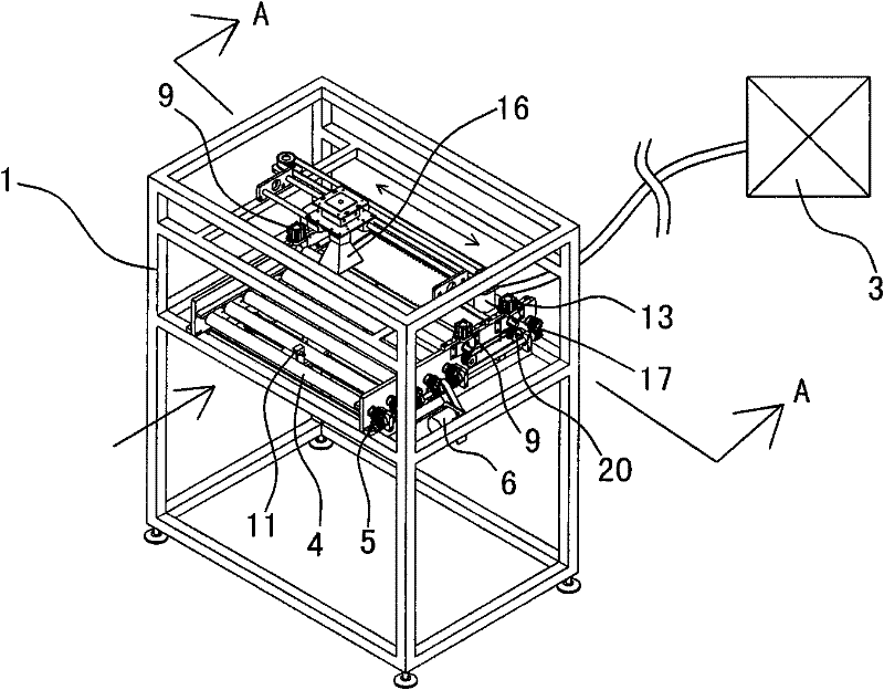
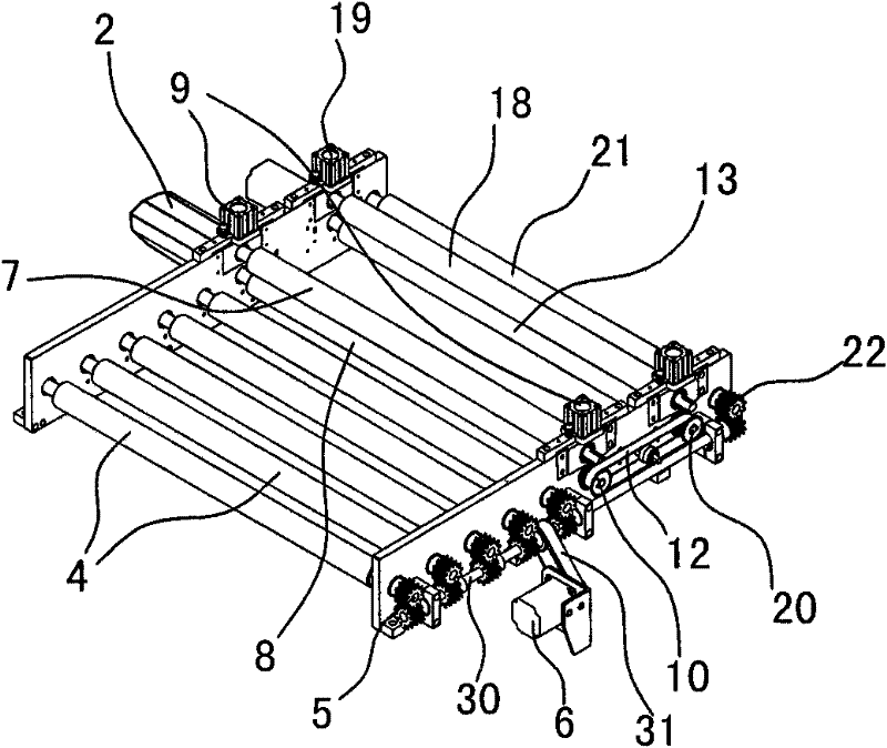
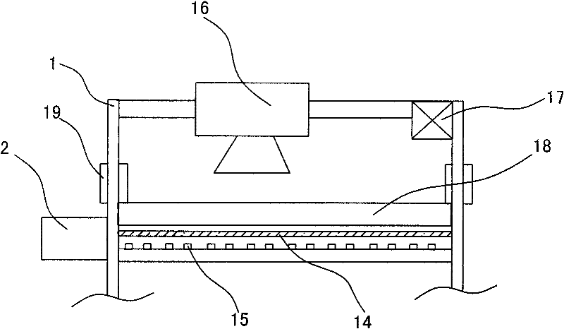
[0019] as attached figure 1 , attached figure 2 and attached image 3 As shown, this embodiment discloses an automatic inspection device for PCB circuit board defects. The automatic inspection device for PCB circuit board defects includes a frame 1, and the frame 1 is sequentially provided with a group of horizontally arranged board feeding rollers, a board feeding Pressure roller group, position detection switch 11 for detecting the position of PCB circuit board, detection light source mechanism, camera device, plate output pinch roller group, horizontally arranged plate output roller group and power device 2, the PCB circuit board defects are automatically inspected The equipment also includes a computer 3 with defect analysis, inspection and control programs; horizontally arranged board feeding rollers, board feeding pinch rollers, position detection sw...


PUM


Abstract

The invention discloses an apparatus for automatically inspecting defects of PCB (printed circuit board), comprising a frame, wherein a horizontally-arranged board feeding roller group, a board feeding compacting roller group, a position detecting switch, a light source detecting mechanism, a camera device, a board exit compacting roller group, a horizontally-arranged board exit roller group and a power device are arranged on the frame; the horizontally-arranged board feeding roller group is connected with a computer with a detecting and controlling program and is operated under the control of the computer; the position detecting switch is used for detecting the PCB; in use, the board feeding compacting roller group and the board exit compacting roller group act sequentially to send the PCB to be photographed gradually by the camera device, then the photographed images are spliced into an image by the computer, and the computer conducts comparison and operational analysis on the spliced image and a standard image prepared in advance so as to find the defect; furthermore, the outside of the defects are surrounded by lines of different colors and the serial number of the board is marked so that the board can be searched and repaired. The apparatus has a simple structure, smart concept, high automation, high inspection efficiency, high detection veracity, convenience in operationand low manufacturing cost, and is suitable for general popularization and application.

Description

technical field [0001] The invention relates to the technical field of product defect inspection machinery manufacturing, in particular to a fully automatic inspection device for PCB circuit board defects. Background technique [0002] At present, a large part of product defect inspection in the PCB circuit board production process relies on manual visual inspection, and the other part is inspected by machinery. When using mechanical inspection, most of them are compared with the correct circuit board image obtained by line scanning, and the computer automatically analyzes and finds out the inspection method of circuit board defects. Compared with manual inspection, the inspection accuracy is greatly improved. improve. However, the operator needs to put the PCB circuit board to be inspected on the inspection table, and after manually marking the detected defect position, manually take it out and enter the next repair process. This kind of mechanical inspection relies on ma...

Claims


Application Information

Patent Timeline
IPC IPC(8): G01N21/956
Inventor 肖开文
Owner MEIZHOU TAIYUAN TECH
Why Eureka
Try Eureka