Ultrasonic bonding method and special ultrasonic welding machine used for optoelectronic device packaging

A photoelectric device and ultrasonic technology, applied in the direction of electric solid devices, electrical components, semiconductor devices, etc., can solve the problems of complex equipment structure, high packaging cost, high equipment cost, etc., to ensure packaging quality, improve service life, and reduce stress concentration Effect

Active Publication Date: 2011-10-26
SHANGHAI UNIV
View PDF1 Cites 21 Cited by
  • Summary
  • Abstract
  • Description
  • Claims
  • Application Information

AI Technical Summary

Problems solved by technology

Ultrasonic packaging technology is widely used in the bonding of polymer materials and metal materials, and has made important research progress, but the bonding equipment has a complex structure, high equipment cost, and is not easy to control
Especially in the field of optoelectronic device packaging technology, the operation is relatively complicated, the packaging cost is high, and the precision of the packaging production line needs to be further improved

Method used


Image

  • Ultrasonic bonding method and special ultrasonic welding machine used for optoelectronic device packaging
  • Ultrasonic bonding method and special ultrasonic welding machine used for optoelectronic device packaging
  • Ultrasonic bonding method and special ultrasonic welding machine used for optoelectronic device packaging

Examples


Embodiment Construction

[0038] In conjunction with accompanying drawing, preferred embodiment of the present invention is described in detail as follows:

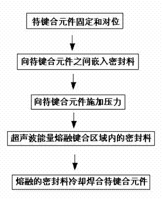
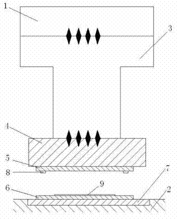
[0039] see Figure 1 ~ Figure 3 , the ultrasonic bonding method that the present invention is used for optoelectronic device packaging comprises the steps:

[0040] a. Fix and accurately align the glass cover plate 5 and the glass substrate 6 to be bonded by using the clamping member;

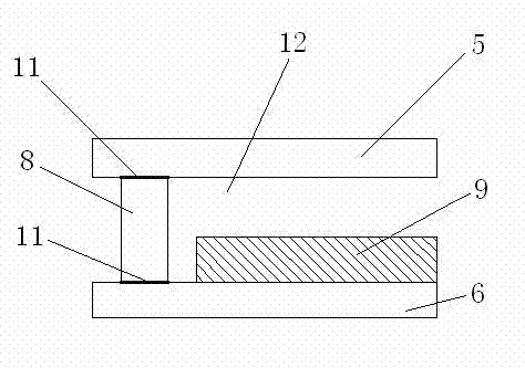
[0041] b. Insert glass sealant between the glass cover plate 5 and the glass substrate 6 in step a, the glass sealant embeds the gap between the glass cover plate 5 and the glass substrate 6, and forms a glass seal 8, the glass cover plate 5 The bonding surface area 11 that forms direct contact with the glass substrate 6 and the glass seal 8 respectively;

[0042] c. Apply initial pressure to the glass cover plate 5 and glass substrate 6 in step b, so that the glass cover plate 5 and glass substrate 6 clamp the glass seal 8;

[0043] d. Utilize the ultrasonic ge...


PUM


Abstract

The present invention discloses an ultrasonic bonding method and a special ultrasonic welding machine used for optoelectronic device packaging. The ultrasonic bonding method provided by the invention comprises the following steps of: fixing and precisely positioning the component to be welded, and applying an initial clamping force on the component to be welded, so that a glass sealing material is clamped by the component to be welded; and transferring the high-frequency vibration energy generated by an ultrasonic welding machine to the bonding surfaces through an energy guiding component, thus realizing the indeformable rapid welding package of the component to be welded. The special ultrasonic welding machine provided by the invention comprises an ultrasonic generator, a clamping component, the energy guiding component and a temperature control device. The ultrasonic bonding method and the special ultrasonic welding machine provided by the invention can accurately and precisely utilize energy, achieve the hermetic package of the component to be welded through energy transfer and transformation, significantly improve the residual stress distribution of the semiconductor optoelectronic device packaging layer, reduce stress concentration, guarantee the packaging quality of the semiconductor optoelectronic device and prolong the service life of the optoelectronic device, and canbe widely applied in the packaging of OLEDs (organic light emitting diodes), solar cells and other semiconductor optoelectronic devices.

Description

technical field [0001] The invention relates to an ultrasonic bonding method and a special ultrasonic welding machine for optoelectronic device packaging, which are suitable for the packaging of organic light emitting diode (OLED) displays, solar cells and other optoelectronic devices, and belong to the technical field of optoelectronic device packaging technology and equipment . Background technique [0002] In recent years, with the continuous development of optoelectronic device technology, ordinary LEDs, OLEDs, and solar cells have entered the public's sight, and are widely considered to be one of the most promising display technologies. Among them, OLED has the advantages of high brightness, good color contrast, wide viewing angle, fast refresh rate and low energy consumption. However, the organic light-emitting layer and electrodes in the OLED device are very sensitive to oxygen and moisture in the surrounding environment, and will interact with it to degrade, thus gr...

Claims


Application Information

Patent Timeline
Patent Type & Authority Applications(China)
IPC IPC(8): C03B23/24H01L51/56
Inventor 张建华李懋瑜赖禹能黄元昊陈遵淼
Owner SHANGHAI UNIV
Why Eureka
Try Eureka