

Multilayer stacked inductance utilizing parallel connection of metals
A multi-layer stacking and metal technology, applied in the field of microelectronics, can solve the problem of low quality factor, achieve high inductance quality factor, and increase the effect of inductance value
- Summary
- Abstract
- Description
- Claims
- Application Information
AI Technical Summary
Problems solved by technology
Method used
Image

Examples
Embodiment Construction
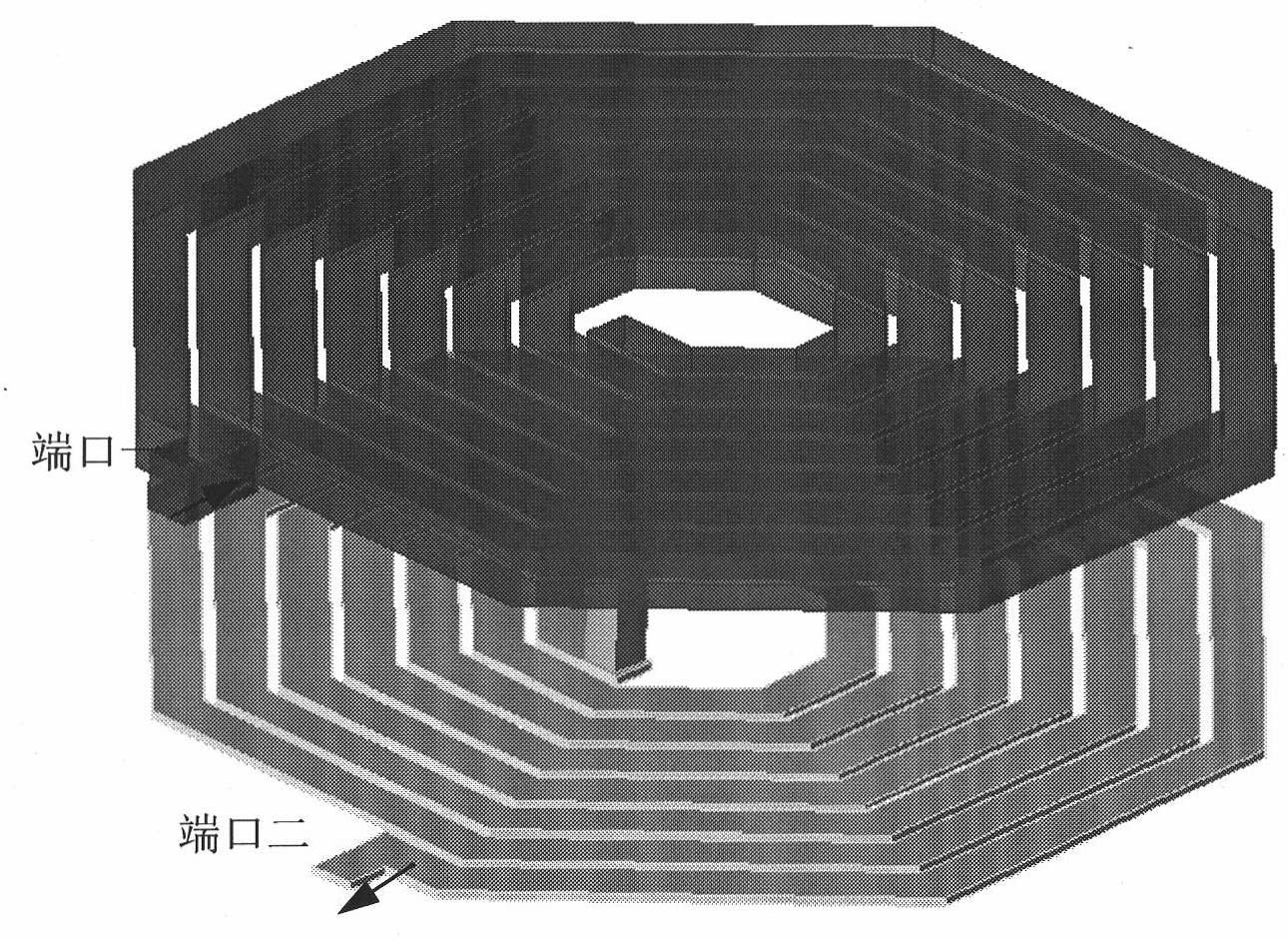
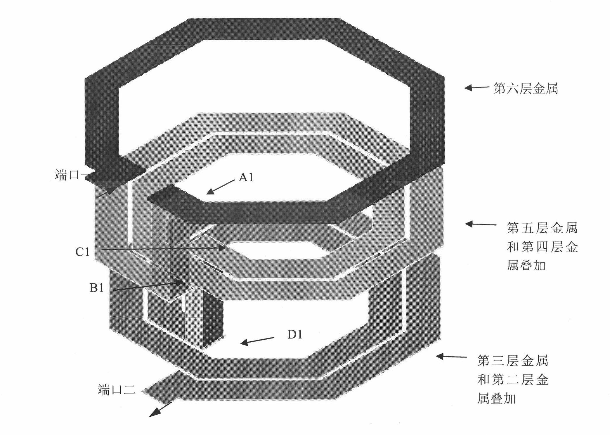
[0015] A multi-layer stacked inductance using metal in parallel according to the present invention; it is a multi-layer structure, including: at least three layers of metal coils on the upper and lower sides, and the slotted parts of the metal coil patterns are aligned; the other metal coils except the top metal coil The lower layer metal coils are formed by stacking and connecting multiple layers of metal; the multiple layers of metal coils are interconnected by strip-shaped through holes.
[0016] In more detail, the multi-layer stacked inductors using metal parallel connection described in the present invention, from figure 2 It can be seen that the metal widths of the upper and lower layers of inductors are the same, from figure 2 It can be seen from the perspective view that the structure of the present invention has three upper and lower layers of metal coils, and the grooved parts of the metal coil patterns are aligned; the other lower layer metal coils except the top...
PUM
 Abstract
Description
Claims
Application Information