Array substrate and manufacturing method thereof and liquid crystal display

A technology of array substrate and substrate substrate, which is applied in semiconductor/solid-state device manufacturing, instruments, electric solid-state devices, etc., can solve the problems of large influence of pixel unit aperture ratio, image signal transmission, and reduction of light transmission area, etc. Achieving good display quality, increasing storage capacitance value, and small resistance-capacitance delay

Active Publication Date: 2011-11-09
BEIJING BOE OPTOELECTRONCIS TECH CO LTD
View PDF5 Cites 34 Cited by
  • Summary
  • Abstract
  • Description
  • Claims
  • Application Information

AI Technical Summary

Problems solved by technology

[0006] However, the formation of these two storage capacitors has certain defects: based on the storage capacitor of the gate line, there is a large parasitic capacitance between the pixel electrode and the gate line, resulting in a relatively large resistance-capacitance delay (RC Delay), which will affect the image signal. Transmission; based on the storage capacitance of the common electrode line, in order to achieve a certain capacitance value, it must ensure that there is a large enough overlapping area, and the opaque common electrode line will reduce the light-transmitting area in the pixel unit, so the pixel unit The opening ratio of the

Method used


Image

  • Array substrate and manufacturing method thereof and liquid crystal display
  • Array substrate and manufacturing method thereof and liquid crystal display
  • Array substrate and manufacturing method thereof and liquid crystal display

Examples


Embodiment 1

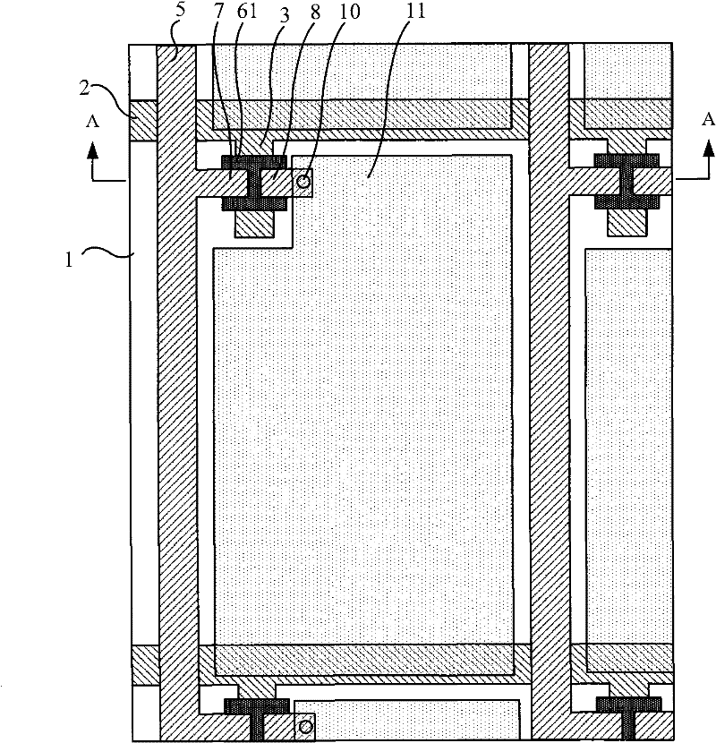
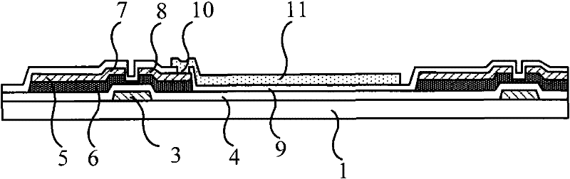
[0044] Figure 3A It is a schematic diagram of a partial top view structure of the array substrate provided in Embodiment 1 of the present invention, Figure 3B for Figure 3A Schematic diagram of the cross-sectional structure in side view along the line C-C. Such as Figure 3A and 3BAs shown, the array substrate includes a base substrate 1; the base substrate 1 is formed with data lines 5 and gate lines 2 that cross vertically and horizontally; the data lines 5 and gate lines 2 surround pixel units arranged in a matrix; each The pixel unit includes a TFT switch and a pixel electrode 11; the TFT switch includes a gate electrode 3, a source electrode 7, a drain electrode 8 and an active layer 6; the gate electrode 3 is connected to the gate line 2, the source electrode 7 is connected to the data line 5, and the drain electrode 8 is connected to The pixel electrode 11 , the active layer 6 are formed between the source electrode 7 and the drain electrode 8 and the gate electr...

Embodiment 2

[0051] Figure 4 The partial top-view structural diagram of the array substrate provided by Embodiment 2 of the present invention. The difference between this embodiment and Embodiment 1 is that the additional electrode 13 on each gate line 2 is connected to the common electrode line in two adjacent pixel units. 12 electrical connections. This technical solution can be realized simply by appropriately changing the number and position of the additional via holes, and changing the pattern of the jumper wire 16 .

[0052] The technical solution of this embodiment can not only optimize the storage capacitance, but also connect the adjacent common electrode lines formed in rows through additional electrodes, so as to avoid storing common voltage differences between the common electrode lines of each row, and make the common voltage uniformity in the common electrode lines better. High, this can avoid the flickering phenomenon that occurs in the display process of the pixel unit. ...

Embodiment 3

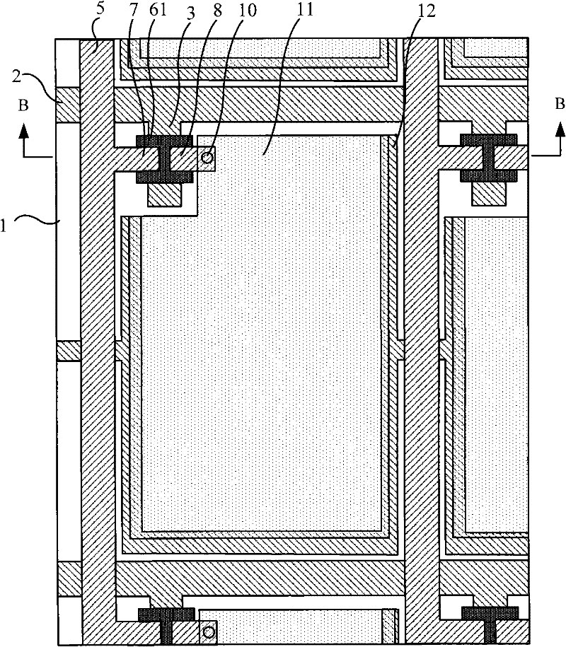
[0054] Figure 5A It is a schematic diagram of a partial top view structure of the array substrate provided in Embodiment 3 of the present invention, Figure 5B for Figure 5A Schematic diagram of the cross-sectional structure in side view along the line D-D. The difference between the technical solution of this embodiment and the first embodiment is that: the common electrode lines 12 and the data lines 5 are formed in the same layer and the patterns are spaced apart from each other, and the additional electrodes 13 and the common electrode lines 12 are integrally formed.

[0055] The technical solution of this embodiment still has the advantage of increasing the storage capacitance, and can reduce the area of ​​the common electrode line under the premise of forming the same storage capacitance value, thereby increasing the aperture ratio of the pixel unit. In addition, compared with the technical solution of the first embodiment, this embodiment also omits the process of f...


PUM


Abstract

The invention discloses an array substrate and a manufacturing method thereof and a liquid crystal display. In the array substrate, an additional electrode is formed above a grid line, the additional electrode and the grid line are mutually spaced by virtue of a grid insulating layer, and the additional electrode is electrically connected with a public electrode wire; a pattern of a pixel electrode extends to the upward side of the additional electrode to be overlapped with the additional electrode, and overlapped parts of the pixel electrode, the additional electrode and the public electrodewire form a storage capacitor. According to the invention, two forms of a grid line-based storage capacitor and a public electrode wire-based storage capacitor are combined, storage capacitance can be improved, and influence of the storage capacitor on other display factors is reduced, aperture opening ratio is not reduced as an overlarge public electrode wire area is required, resistance-capacitance delay is shorter, and better display quality can be obtained.

Description

technical field [0001] The invention relates to liquid crystal display technology, in particular to an array substrate, a manufacturing method thereof and a liquid crystal display. Background technique [0002] A liquid crystal display is a commonly used flat panel display at present, and a thin film transistor liquid crystal display (ThinFilm Transistor Liquid Crystal Display, TFT-LCD for short) is a mainstream product in the liquid crystal display. [0003] The liquid crystal panel is an important part of TFT-LCD, and generally includes an array substrate and a color filter substrate arranged in opposite cells, and a liquid crystal layer is filled between them. Figure 1A is a partial top view structural schematic diagram of an existing array substrate, Figure 1B for Figure 1A Schematic diagram of the cut-away structure in side view along line A-A. Such as Figure 1A and 1B As shown, the array substrate includes a base substrate 1; the base substrate 1 is formed with d...

Claims


Application Information

Patent Timeline
Patent Type & Authority Applications(China)
IPC IPC(8): G02F1/1362H01L27/02H01L21/77
CPCG02F1/136213G02F1/1343G02F1/136286
Inventor 谢振宇陈旭龙春平徐少颖
Owner BEIJING BOE OPTOELECTRONCIS TECH CO LTD
Why Eureka
Try Eureka