
Semiconductor laser and manufacturing method thereof

A semiconductor and laser technology, applied in the field of semiconductor lasers and their manufacturing, can solve problems such as cavity surface degradation and degradation, and achieve the effect of improving reliability and saving lithography steps.

Inactive Publication Date: 2011-11-09
RENESAS ELECTRONICS CORP
View PDF5 Cites 7 Cited by
  • Summary
  • Abstract
  • Description
  • Claims
  • Application Information

AI Technical Summary

Problems solved by technology

[0005] Major degradation factors of blue-violet LDs using GaN include stepwise degradation, in which the active layer is degraded due to current supply in the same manner as GaAs and InP type lasers; and catastrophic optical degradation (COD), in which the cavity face unexpectedly deteriorated

Method used


Image

  • Semiconductor laser and manufacturing method thereof
  • Semiconductor laser and manufacturing method thereof
  • Semiconductor laser and manufacturing method thereof

Examples


Embodiment Construction

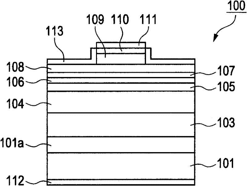
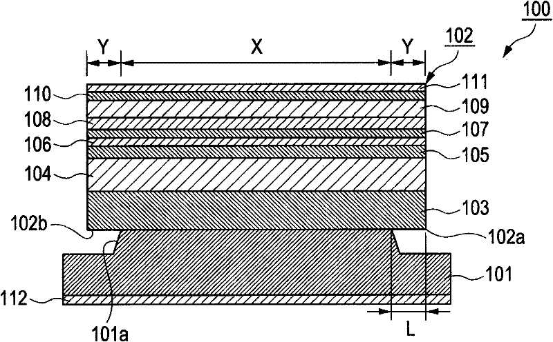
[0027] In a preferred embodiment, the semiconductor substrate has a recessed region below the facet of the resonator, such that the semiconductor substrate does not contact the resonator.

[0028] In a preferred embodiment, the recessed area corresponds to the location of the non-current injection area and the window area for the resonator.

[0029] In a preferred embodiment, the resonator has a lower cladding layer and an active layer formed over the lower cladding layer. A length from an end surface of a region not in contact with the semiconductor substrate at the lower surface of the resonator is smaller than the thickness of the lower cladding layer.

[0030] In a preferred embodiment, the length from the end face of the region at the lower surface of the resonator not in contact with the semiconductor substrate is less than 20 μm.

[0031] In a preferred embodiment, the semiconductor laser also has a first electrode electrically coupled to the resonator and a second ele...


PUM


Abstract

The invention provides a semiconductor laser and a manufacturing method thereof. The semiconductor laser includes a semiconductor substrate and a resonator formed over the semiconductor substrate and containing a nitride semiconductor layer. A strain exerting on a region near the facet of the resonator is smaller than a strain exerting on the region between the regions near the facet.

Description

[0001] Cross References to Related Applications [0002] The entire disclosure of Japanese Patent Application No. 2010-98650 filed on April 22, 2010 including specification, claims, drawings and abstract is incorporated herein by reference in its entirety. technical field [0003] The present invention relates to a semiconductor laser and a method of manufacturing the same, for example, a semiconductor laser having a nitride semiconductor layer and a method of manufacturing the same. Background technique [0004] Group III element nitride semiconductors generally represented by gallium nitride (GaN) have been focused on as materials for light emitting diodes (LEDs) or laser diodes (LDs) because they can emit blue-violet with high efficiency. Among them, LDs of the 405 nm band are expected as light sources for large-capacity optical disc devices because they can further confine light beams compared with existing LDs of the 650 nm band. In recent years, with the spread of wid...

Claims


Application Information

Patent Timeline
Patent Type & Authority Applications(China)
IPC IPC(8): H01S5/16
CPCH01S5/3201H01S5/16B82Y20/00H01S5/22H01S5/021H01S5/0207H01S2301/176H01S2301/173H01S5/0203H01S5/34333
Inventor 笹冈千秋
Owner RENESAS ELECTRONICS CORP
Learn More