Nano silicon thin film transistor pressure sensor

A nano-silicon film and pressure sensor technology, applied in the field of sensors, can solve the problems of pressure sensor zero drift and other problems, and achieve the effects of zero drift compensation, high sensitivity, and good temperature stability

Active Publication Date: 2013-01-30
涿州方方电子科技有限公司
View PDF4 Cites 0 Cited by
  • Summary
  • Abstract
  • Description
  • Claims
  • Application Information

AI Technical Summary

Problems solved by technology

[0003] The purpose of the present invention is to solve the problem of zero point drift in the existing pressure sensor, and to provide a nano-silicon thin film transistor pressure sensor

Method used


Image

  • Nano silicon thin film transistor pressure sensor
  • Nano silicon thin film transistor pressure sensor
  • Nano silicon thin film transistor pressure sensor

Examples


specific Embodiment approach 1

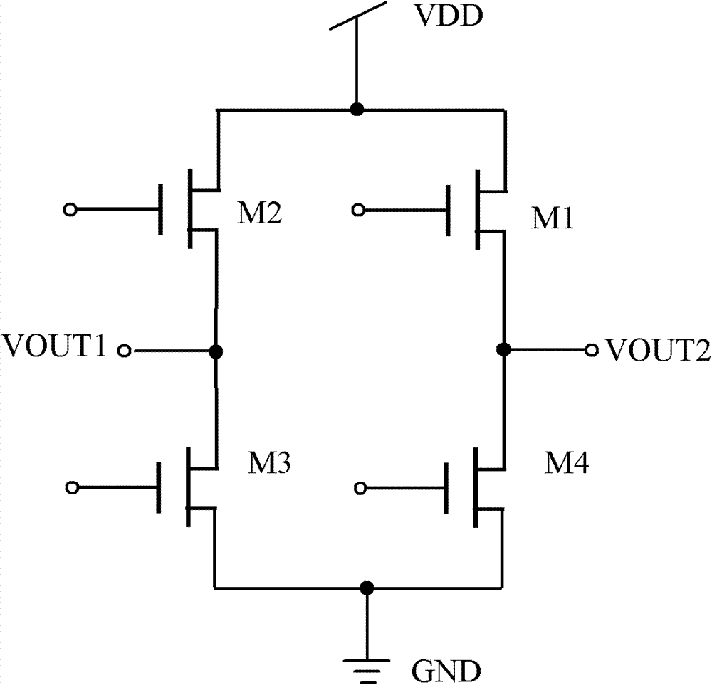
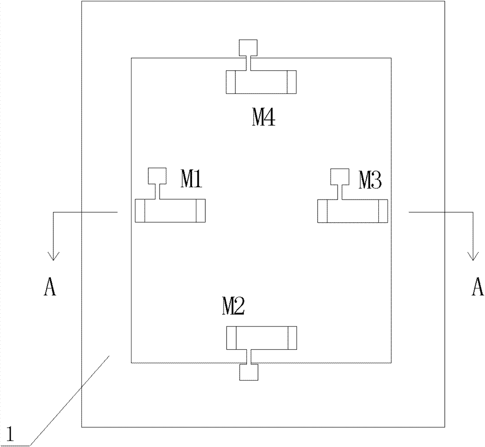
[0016] Specific implementation mode one: the following combination Figure 1 to Figure 6 This embodiment mode is described. This embodiment mode is composed of a first nano-silicon thin film transistor M1, a second nano-silicon thin film transistor M2, a third nano-silicon thin film transistor M3, a fourth nano-silicon thin film transistor M4 and a single crystal silicon substrate 1.

[0017] The source of the first nanometer silicon thin film transistor M1 is connected to the drain of the fourth nanometer silicon thin film transistor M4, the drain of the first nanometer silicon thin film transistor M1 is connected to the drain of the second nanometer silicon thin film transistor M2, and the second nanometer silicon thin film transistor The source of M2 is connected to the drain of the third nanometer silicon thin film transistor M3, and the source of the third nanometer silicon thin film transistor M3 is connected to the source of the fourth nanometer silicon thin film transis...

specific Embodiment approach 2

[0024] Embodiment 2: This embodiment is a further description of Embodiment 1. The single crystal silicon substrate 1 is a p-type double-sided polished single crystal silicon wafer in the crystal orientation. Others are the same as the first embodiment.

specific Embodiment approach 3

[0025] Embodiment 3: This embodiment is a further description of Embodiment 2, and the thickness of the single crystal silicon substrate 1 is 400 microns. Others are the same as the second embodiment.


PUM

PropertyMeasurementUnit
thicknessaaaaaaaaaa
thicknessaaaaaaaaaa

Abstract

The invention discloses a nano silicon thin film transistor pressure sensor, which belongs to the technical field of sensors and solves the problem of zero drift in the current pressure sensor. The nano silicon thin film transistor pressure sensor is composed of a first nano silicon thin film transistor, a second nano silicon thin film transistor, a third nano silicon thin film transistor, a fourth nano silicon thin film transistor and a monocrystal silicon substrate, wherein the drain electrode of the first nano silicon thin film transistor is connected with a power supply VDD; the source electrode of the fourth nano silicon thin film transistor is grounded GND; the lead-out end of the source electrode of the second nano silicon thin film transistor is used as a first output voltage end VOUT1, the lead-out end of the source electrode of the first nano silicon thin film transistor is used as a second output voltage end VOUT2; and the four nano silicon thin film transistors are all arranged on the monocrystal silicon substrate, the back of the monocrystal silicon substrate is of a C-shaped silicon cup structure, and channel resistor structures of the four nano silicon thin film transistors form a Wheatstone bridge structure. The nano silicon thin film transistor pressure sensor is used for pressure detection.

Description

technical field [0001] The invention relates to a nano-silicon thin film transistor pressure sensor, which belongs to the technical field of sensors. Background technique [0002] At present, ultra-micro-pressure pressure sensors are manufactured by designing new silicon membrane structures or new pressure-sensitive materials. Due to sensor structure and process limitations, it is difficult to miniaturize the device size and there is zero drift. Contents of the invention [0003] The purpose of the present invention is to solve the problem of zero point drift in the existing pressure sensor, and provide a pressure sensor of nano-silicon thin film transistor. [0004] The invention consists of a first nanometer silicon thin film transistor, a second nanometer silicon thin film transistor, a third nanometer silicon thin film transistor, a fourth nanometer silicon thin film transistor and a single crystal silicon substrate, [0005] The source of the first nano-silicon thin ...

Claims


Application Information

Patent Timeline
Patent Type & Authority Patents(China)
IPC IPC(8): G01L9/06B82Y15/00
Inventor 赵晓锋温殿忠庄萃萃李玥
Owner 涿州方方电子科技有限公司
Why Eureka
Try Eureka