
Semiconductor luminous device

A light-emitting device, semiconductor technology, applied in the direction of semiconductor devices, electric solid state devices, electrical components, etc.

Inactive Publication Date: 2013-01-23
北京宇极芯光光电技术有限公司
View PDF4 Cites 0 Cited by
  • Summary
  • Abstract
  • Description
  • Claims
  • Application Information

AI Technical Summary

Problems solved by technology

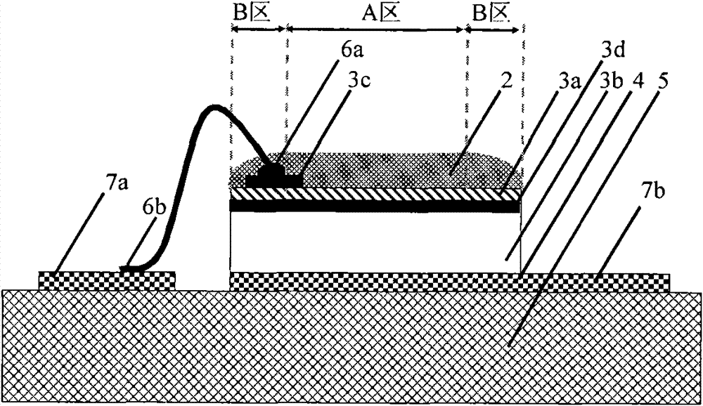
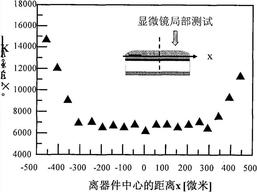
In the end, different positions on the surface of the device have different color temperature distributions, that is, the formation of light spots, which affects the application effect, such as Figure 1c

Method used


Image

  • Semiconductor luminous device
  • Semiconductor luminous device
  • Semiconductor luminous device

Examples


Embodiment 1

[0112] Embodiment 1——Packaging of a glass sheet with a smooth surface placed on a fluorescent glue

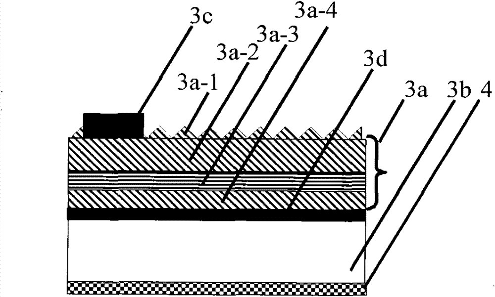
[0113] Prepare 2 AlN packaging substrates with electrode structures and 2 smooth transparent glass sheets (size 1mm2, the same as thinfilm chips, such as Figure 2a ), ultrasonic cleaning in ethanol solution for 3 minutes for surface cleaning. Store the treated glass flakes in a clean place for subsequent use. Paste the thinfilm chip (1mm2,) on the AlN packaging substrate with Au0.8Sn0.2 alloy glue. Place the packaging substrate together with the chip on a heating plate with a set temperature of 340° C. for 30 seconds and then take it off. The alloy glue is melted at high temperature and then cooled and solidified, so that the chip is bonded and fixed on the AlN substrate. The chip and the AlN substrate were soaked in an acetone organic solution and ultrasonically cleaned for 3 minutes to remove the waxy adhesive on the alloy surface. Electrode welding is performed with a g...

Embodiment 2

[0115] Example 2 - Glass flake with tiny protrusions on one side

[0116] Prepare two AlN packaging substrates with electrode structures and two transparent glass flakes with tiny protrusions on one side (size 1mm2, the same as thinfilm chips), and ultrasonically clean them in ethanol solution for 3 minutes for surface cleaning. After treatment, the tiny convex surface on the side of the transparent glass sheet presents a smooth curved shape, and the height of the convex is about 400 μm, which is greater than the height of the arc of the gold wire, such as Figure 3a . Store the treated glass flakes in a clean place for subsequent use. Paste the thinfilm chip (1mm2,) on the AlN packaging substrate with Au0.8Sn0.2 alloy glue. Place the packaging substrate together with the chip on a heating plate with a set temperature of 340° C. for 30 seconds and then take it off. The alloy glue is melted at high temperature and then cooled and solidified, so that the chip is bonded and fi...

Embodiment 3

[0120] Example 3 - Combination of transparent beads mixed with fluorescent glue and smooth glass sheet

[0121] Prepare 2 AlN packaging substrates with electrode structures and 2 transparent glass flakes with a smooth surface (size 1mm2, the same as the thinfilm chip), and ultrasonically clean them in ethanol solution for 3 minutes to clean the surface. Store the treated glass flakes in a clean place for subsequent use. Paste the thinfilm chip (1mm2,) on the AlN packaging substrate with Au0.8Sn0.2 alloy glue. Place the packaging substrate together with the chip on a heating plate with a set temperature of 340° C. for 30 seconds and then take it off. The alloy glue is melted at high temperature and then cooled and solidified, so that the chip is bonded and fixed on the AlN substrate. The chip and the AlN substrate were soaked in an acetone organic solution and ultrasonically cleaned for 3 minutes to remove the waxy adhesive on the alloy surface. Electrode welding is performe...


PUM


Abstract

The invention relates to a "semiconductor light-emitting device" and belongs to the field of light-emitting diodes. A transparent glass sheet is placed on the upper part of the fluorescent glue after dispensing, so that the thickness of the fluorescent glue film on the surface of the device remains uniform. The use of a transparent support between the glass sheet and the light-emitting device solves the problem of large color temperature differences between different packaging devices. The invention can realize the uniformity of the color temperature of a single package device in the simplest way, improve the light spot of the device, and the consistency of the color temperature among different devices, and improve the production efficiency.

Description

technical field [0001] The invention relates to a packaging method of a semiconductor light-emitting device with a light-emitting diode chip coated with fluorescent powder resin (silica gel). The function of the phosphor layer is to absorb the light emitted by part of the LED chips for conversion, and work together with the light emitted by the remaining chips to change the luminous color of the device. The function of the invention is to reduce the inhomogeneity of the luminous color caused by the uneven distribution of fluorescent substances on the surface of the chip, and especially can be used to improve the yield of white light sources of light-emitting diodes. Background technique [0002] Light Emitting Diode (LED, Light Emitting Diode, is a semiconductor solid light-emitting device, which has significant advantages such as long life, energy saving, safety, green environmental protection, pure light color, small size, etc. Monochromatic light. Therefore, when making ...

Claims


Application Information

Patent Timeline
Patent Type & Authority Patents(China)
IPC IPC(8): H01L33/48H01L33/50H01L33/56H01L33/36
CPCH01L2224/45144H01L2224/48091H01L2224/48465H01L2224/48471H01L2224/48479H01L2224/8592H01L2924/00014
Inventor 王海嵩鲍鹏
Owner 北京宇极芯光光电技术有限公司
Learn More