Packaging structure and method of high-power LED

A LED packaging and high-power technology, applied in the direction of electrical components, circuits, semiconductor devices, etc., can solve the problems of inconsistent color temperature of light source space, lower product reliability, inconsistent thickness, etc., to achieve uniformity, improve reliability, improve The effect of adhesion

Inactive Publication Date: 2011-03-02
UNILUMIN GRP
View PDF6 Cites 14 Cited by
  • Summary
  • Abstract
  • Description
  • Claims
  • Application Information

AI Technical Summary

Problems solved by technology

This packaging method has at least the following disadvantages: 1. Since the glue with phosphor powder is directly dotted around the chip, the thickness of the phosphor glue is inconsistent and the distribution of phosphor powder is uneven, which will lead to different light output from each surface of the chip, which will eventually Inconsistent spatial color temperature of the entire light source
2. Since the fluorescent powder will precipitate, there will be a layer of fluorescent powder on the contact surface of the colloid and the concave cup, which will reduce the adhesion between the colloid and the bracket or the substrate. When the LED is on for a long time, the gap between the colloid and the bracket or the substrate There will be delamination between them, which will reduce the reliability of the product; 3. The direct contact between the phosphor powder and the chip with high heat generation will also reduce the reliability of the product, and the light attenuation is relatively large

Method used


Image

  • Packaging structure and method of high-power LED
  • Packaging structure and method of high-power LED
  • Packaging structure and method of high-power LED

Examples


Embodiment Construction

[0009] The embodiments of the present invention will be further described in detail below in conjunction with the accompanying drawings.

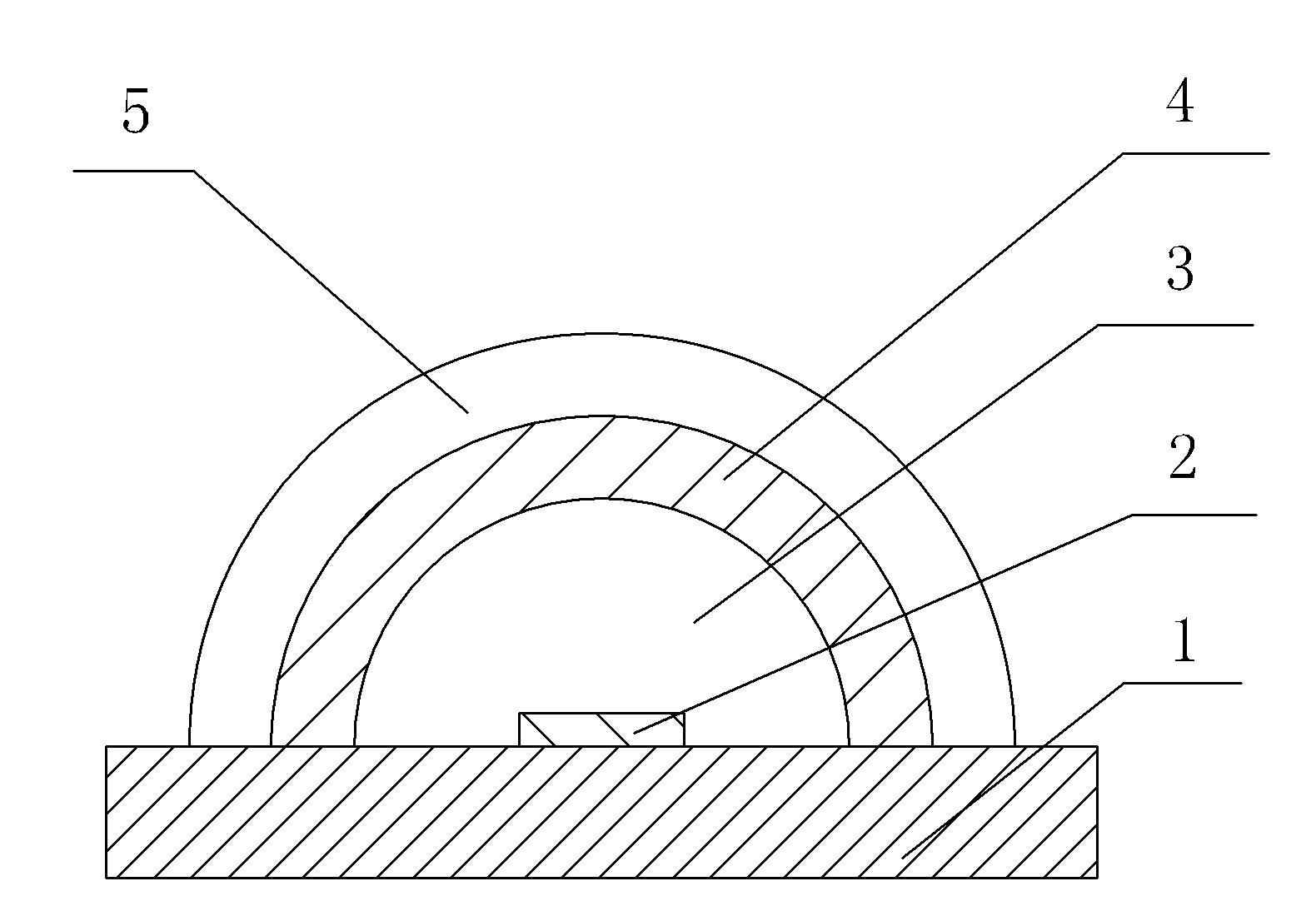
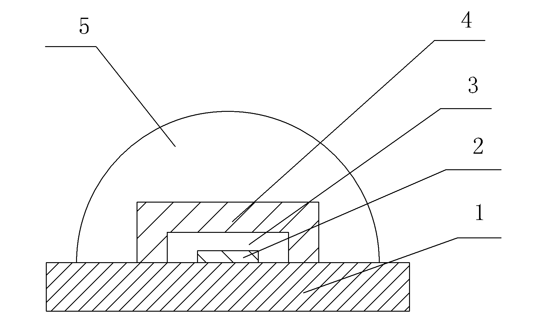
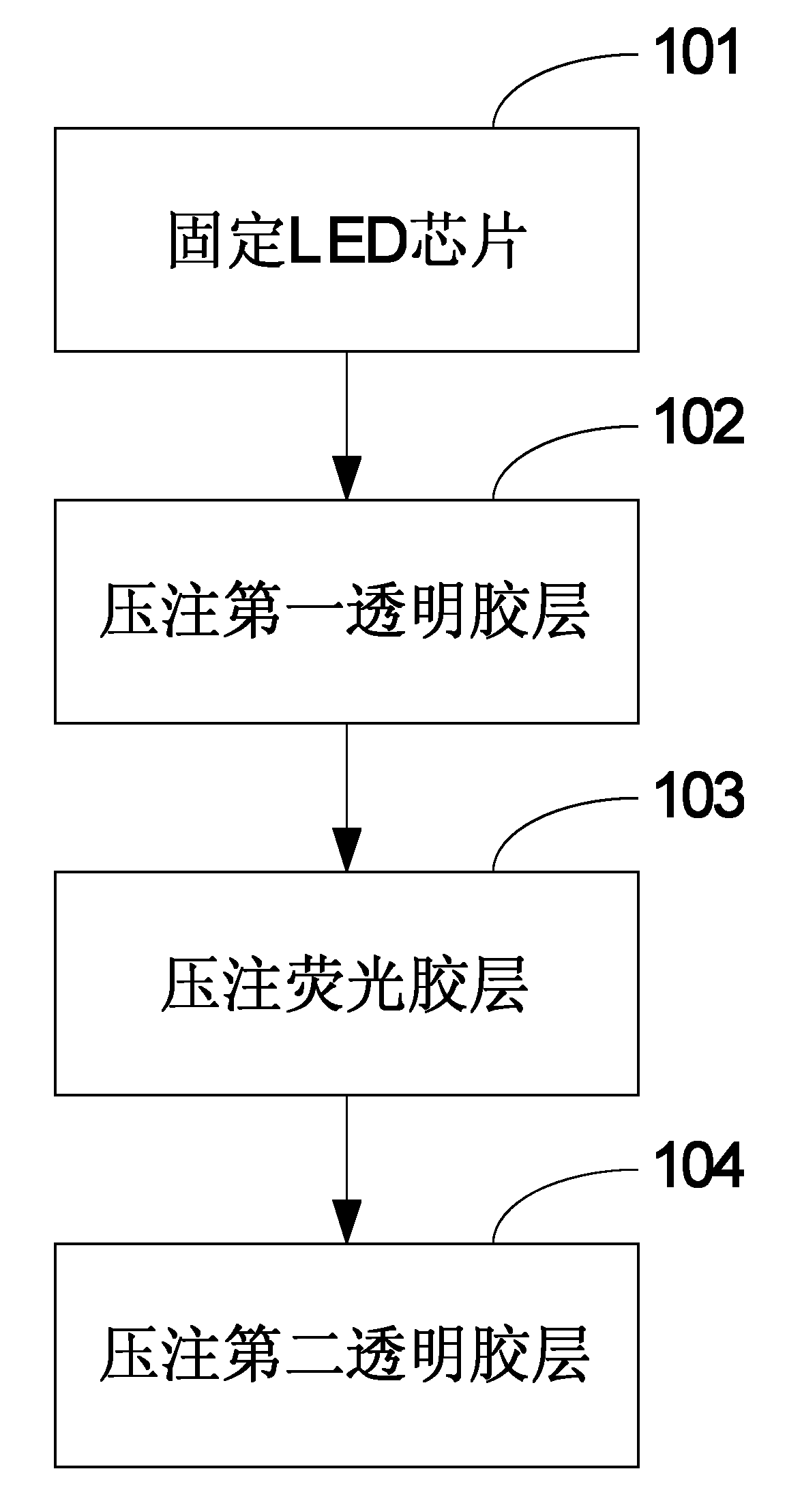
[0010] figure 1 and figure 2 It is a schematic diagram of two embodiments of the high-power LED packaging structure of the present invention. The high-power LED packaging structure provided by the embodiment of the present invention includes: a substrate 1 , an LED chip 2 , a first transparent adhesive layer 3 , a fluorescent adhesive layer 4 and a second transparent adhesive layer 5 .

[0011] Among them, the LED chip 2 is fixed on one side of the substrate 1; the first transparent adhesive layer 3 is a layer of transparent adhesive formed by pressing the LED chip 2 as the center. In this embodiment, the first transparent adhesive layer 3 is pressed by silica gel Injection molding, the refractive index of the first transparent adhesive layer 3 is greater than 1.41, and the hardness is greater than shore A 50; the fluorescent adhesive la...


PUM


Abstract

The embodiment of the invention relates to a packaging structure of high-power LED, comprising a substrate, an LED chip fixed at one side of the substrate, a first transparent adhesive layer formed by pressure injection with the LED chip as the center, a fluorescent adhesive layer formed by pressure injection outside the first transparent adhesive layer and a second transparent adhesive layer formed by pressure injection outside the fluorescent adhesive layer. The embodiment of the invention also provides a packaging method of the high-power LED. The invention has the following beneficial effects: in the method, the fluorescent adhesive layer is formed by a specific die through pressure injection and has uniform thickness; the uniformity and consistency of the color temperature of the light space can be well realized by controlling the shape and thickness of the fluorescent adhesive layer and the fluorescent powder inside the fluorescent adhesive layer to be uniformly distributed; and the first transparent adhesive layer is arranged between the fluorescent adhesive layer and the LED chip and the substrate through pressure injection, thus overcoming the defects of low product reliability and greater light attenuation caused by direct contact between the fluorescent powder and the LED chip with high heat productivity and the substrate.

Description

technical field [0001] The invention relates to LED packaging technology, in particular to a high-power LED packaging structure and packaging method. Background technique [0002] The traditional high-power white LED packaging method is to use silver glue to fix the LED chip on the bracket or substrate with a concave cup, then put the glue with phosphor powder into the concave cup, and then inject a layer of transparent glue and bake it. post-forming. This packaging method has at least the following disadvantages: 1. Since the glue with phosphor powder is directly dotted around the chip, the thickness of the phosphor glue is inconsistent and the distribution of phosphor powder is uneven, which will lead to different light output from each surface of the chip, which will eventually The spatial color temperature of the entire light source is inconsistent. 2. Since the fluorescent powder will precipitate, there will be a layer of fluorescent powder on the contact surface of t...

Claims


Application Information

Patent Timeline
Patent Type & Authority Applications(China)
IPC IPC(8): H01L33/48H01L33/50H01L33/54
Inventor 王月飞
Owner UNILUMIN GRP
Why Eureka
Try Eureka