

Wafer-level image sensor module structure with specific focal length and manufacturing method thereof
A technology of image sensor and module structure, applied in image communication, radiation control device, parts of color TV, etc. Improve product yield and prevent stray light
- Summary
- Abstract
- Description
- Claims
- Application Information
AI Technical Summary
Problems solved by technology
Method used
Image

Examples
Embodiment Construction
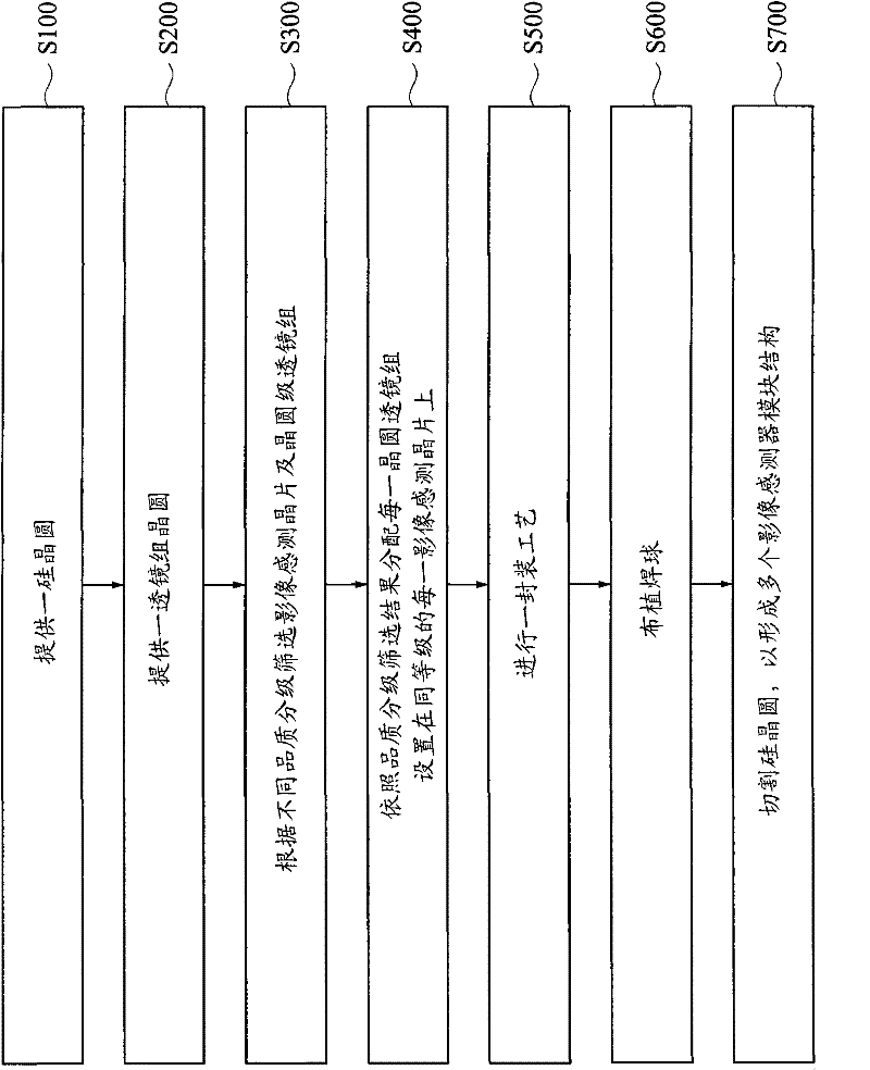
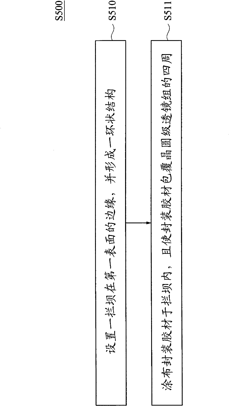
[0056] In order to further explain the technical means and effects of the present invention to achieve the intended purpose of the invention, the structure of the wafer-level image sensor module with a specific focal length and its The specific implementation, method, steps, structure, features and effects of the manufacturing method are described in detail below.
[0057] The aforementioned and other technical contents, features and effects of the present invention will be clearly presented in the following detailed description of preferred embodiments with reference to the drawings. Through the description of the specific implementation mode, a more in-depth and specific understanding of the technical means and effects adopted by the present invention to achieve the intended purpose can be obtained. However, the accompanying drawings are only for reference and description, and are not used to explain the present invention. be restricted.
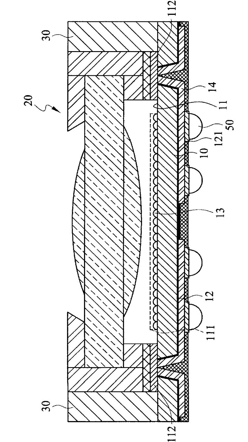
[0058] FIG. 1 is a schematic struc...
PUM
 Abstract
Description
Claims
Application Information