Supercharge Your Innovation With Domain-Expert AI Agents!

Silicon-Based Nanoscale Interleaved Memory

A cross-storage, nanowire technology, applied in the field of solid-state resistance devices, can solve the problems of limited yield, high forming voltage, equipment damage, etc., and achieve the effect of good durability

Active Publication Date: 2016-09-14
RGT UNIV OF MICHIGAN
View PDF6 Cites 0 Cited by
  • Summary
  • Abstract
  • Description
  • Claims
  • Application Information

AI Technical Summary

Problems solved by technology

However, such devices typically have micron-sized filaments, which may prevent them from scaling down to the sub-100nm range
Such devices may also require high forming voltages, which can lead to device damage and limit yield

Method used


Image

  • Silicon-Based Nanoscale Interleaved Memory
  • Silicon-Based Nanoscale Interleaved Memory
  • Silicon-Based Nanoscale Interleaved Memory

Examples


Embodiment Construction

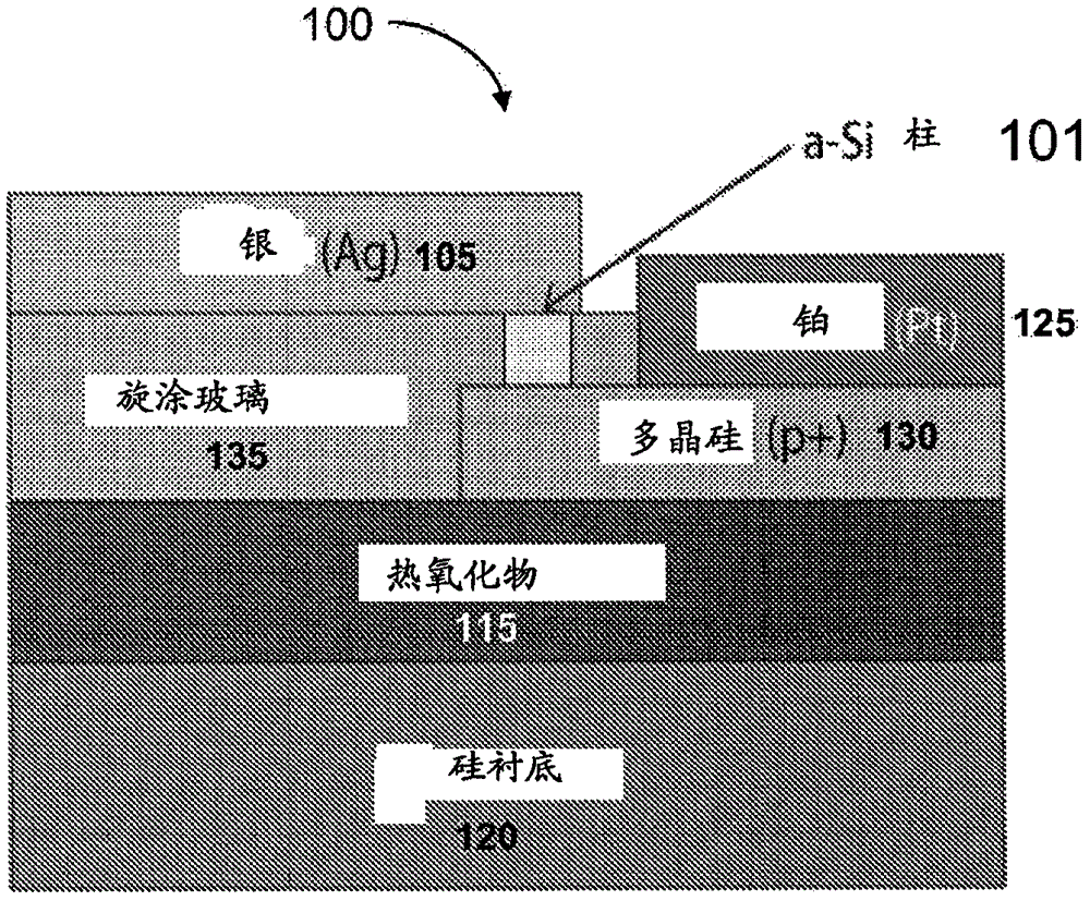
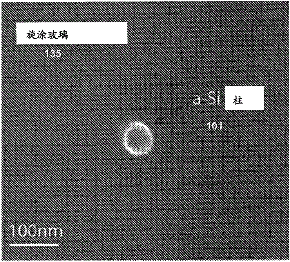
[0037] Figure 1(a) depicts a nonvolatile solid-state resistive device 100 that includes a nanoscale a-Si structure 101 that exhibits a characteristic that can be selectively set to various values ​​and reset. resistors, this is all done with appropriate control circuitry. Once set, the resistance value can be read using a small voltage of sufficient magnitude to determine the resistance without causing it to change. Although the illustrated embodiment uses a-Si as the resistive element, it should be clear that other amorphous silicon (nc-Si) structures can be used, for example, amorphous polycrystalline silicon (sometimes called nanocrystalline silicon, the amorphous phase). Thus, as used herein and in the claims, amorphous silicon (nc-Si) means amorphous silicon (a-Si), amorphous polysilicon (poly-Si) exhibiting controllable resistance, or a combination of both . Furthermore, the illustrated embodiment is an a-Si nanostructure 101 exhibiting Certain properties unique to i...


PUM

PropertyMeasurementUnit
diameteraaaaaaaaaa
diameteraaaaaaaaaa

Abstract

This application describes an interleaved memory array. The interleaved memory array includes a first array of parallel nanowires of a first material and a second array of parallel nanowires of a second material. The first array and the second array are oriented at an angle to each other. The array also includes a plurality of nanostructured amorphous silicon deposited between the nanowires of the first material and the nanowires of the second material at each intersection of the two arrays. The nanostructures together with the nanowires of the first material and the second material form a resistive memory cell.

Description

technical field [0001] The present invention relates to a solid-state resistive device for memory storage. Background technique [0002] Recently, a lot of attention has been paid to resistive random access memory (RRAM) as a potential candidate for ultra-high density non-volatile information storage. A typical RRAM device includes an insulator layer sandwiched between a pair of electrodes and exhibits an electrical pulse-induced resistive hysteresis switching effect. [0003] By virtue of the binary oxides (e.g., NiO and TiQ 2 Joule heating and electrochemical processes in ) or redox processes for ionic conductors including oxides, chalcogenides, and polymers to form conductive filaments within insulators illustrate resistive switching. Also by TiO 2 and field-induced diffusion of ions in amorphous silicon (a-Si) films illustrate resistive switching. [0004] In the case of a-Si structures, the voltage-induced diffusion of metal ions into the silicon results in the form...

Claims


Application Information

Patent Timeline
Patent Type & Authority Patents(China)
IPC IPC(8): H01L27/115H01L21/8247H10N80/00H10N99/00
CPCB82Y10/00G11C13/0011G11C2213/11G11C2213/33G11C2213/77G11C2213/81G11C11/5614H10B63/20H10B63/80H10N70/245H10N70/8416H10N70/884H10N70/063H10N70/826H10B63/82H10N70/20B82Y30/00H10N70/841H10N70/021H10N70/821G11C13/004G11C13/0069G11C13/0097G11C2013/005G11C2013/0071
Inventor 卢伟赵成现金局奂
Owner RGT UNIV OF MICHIGAN
Features
  • R&D
  • Intellectual Property
  • Life Sciences
  • Materials
  • Tech Scout
  • Unparalleled Data Quality
  • Higher Quality Content
  • 60% Fewer Hallucinations
Learn More