

A kind of nitride LED structure and preparation method thereof
A technology of LED structure and nitride, applied in electrical components, circuits, semiconductor devices, etc., can solve the problem of high production cost, and achieve the effects of increasing production cost, improving light extraction efficiency and external quantum effect, and expanding critical angle.
Inactive Publication Date: 2011-12-07
ENRAYTEK OPTOELECTRONICS
View PDF6 Cites 8 Cited by
- Summary
- Abstract
- Description
- Claims
- Application Information
AI Technical Summary
Problems solved by technology
[0007] The purpose of the present invention is to provide a nitride LED structure and its preparation method to solve the problem of high production cost caused by the photolithography process used to form a rough surface on the substrate
Method used
View moreImage
Smart ImageViewing Examples

Examples
preparation example Construction
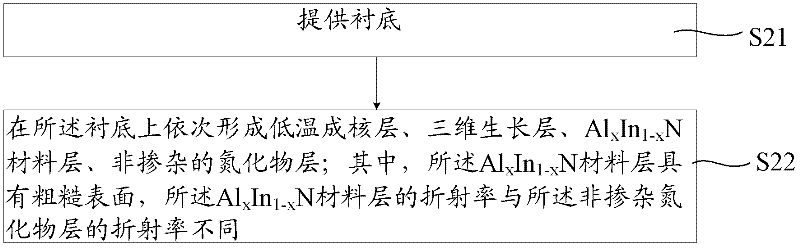
[0037] figure 2 It is a flowchart of the steps of the method for preparing a nitride LED provided in the embodiment of the present invention. refer to figure 2 , the preparation method of the nitride LED structure comprises the following steps:
[0038] S21, providing a substrate;
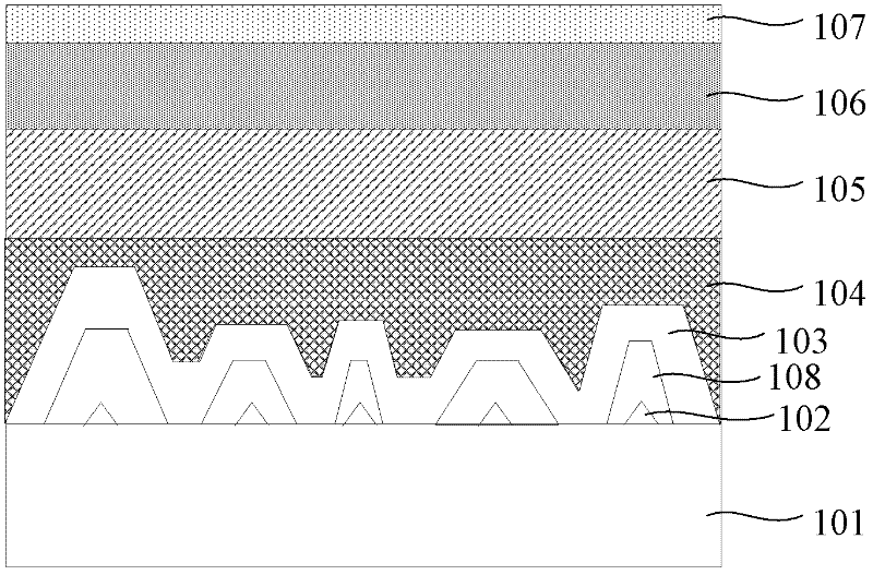
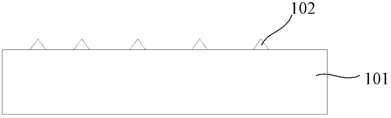
[0039] S22, sequentially forming a low-temperature nucleation layer, a three-dimensional growth layer, and an Al layer on the substrate x In 1-x N material layer, non-doped nitride layer; wherein, the Al x In 1-x The N material layer has a rough surface, the Al x In 1-x The refractive index of the N material layer is different from that of the non-doped nitride layer.
Login to View More PUM
 Abstract
The invention discloses a nitride light emitting diode (LED) structure, which comprises a substrate, a low-temperature nucleation layer and an undoped nitride layer, wherein the low-temperature nucleation layer and the undoped nitride layer grow on the substrate; a three-dimensional growth layer grows on the low-temperature nucleation layer; an AlxIn(1-x)N material layer is arranged between the three-dimensional growth layer and the undoped nitride layer and provided with a rough surface; the refractive index of the AlxIn(1-x)N material layer is different from that of the undoped nitride layer; and the x is more than 0 and less than 1. The invention also provides a preparation method of the nitride LED structure. The nitride LED structure provided by the invention changes the transmissiondirection of light rays due to a scattering effect, expands the critical angle of emergent light, and improves the light extraction efficiency and the external quantum efficiency. The preparation method provided by the invention can be compatible with the ordinary LED epitaxial growth process and is completed in a reaction chamber at one time, and extra machining or processing technologies are not needed.
Description
technical field [0001] The invention relates to the technical field of LED preparation, in particular to a nitride LED structure and a preparation method thereof. Background technique [0002] A light-emitting diode (LED, Light Emitting Diode) is a semiconductor solid-state light-emitting device, which uses a semiconductor PN junction as a light-emitting material, and can directly convert electricity into light. When a forward voltage is applied to both ends of the semiconductor PN junction, the minority carriers injected into the PN junction recombine with the majority carriers, releasing excess energy to cause photon emission, and the direct emission colors are red, orange, yellow, Green, blue, blue, purple light. [0003] With the development of nitride-based high-brightness LED applications, a new generation of green and environmentally friendly solid-state lighting sources-nitride LEDs has become the focus of attention. Group III nitride semiconductor materials mainly...
Claims
Login to View More Application Information
Patent Timeline
 IPC IPC(8): H01L33/20H01L33/32H01L33/00
Inventor于洪波肖德元程蒙召张汝京
OwnerENRAYTEK OPTOELECTRONICS