
A kind of white light led packaging structure and packaging method
A technology of LED packaging and white light, which is applied in the direction of electrical components, electric solid devices, circuits, etc., can solve the problems of uniform mixing of phosphor powder resin, affecting the light efficiency of LED devices, and affecting the uniformity of white light, so as to simplify the packaging process and improve Light efficiency and uniformity of white light, which is beneficial to the effect of device light efficiency and uniformity of white light
- Summary
- Abstract
- Description
- Claims
- Application Information
AI Technical Summary
Problems solved by technology
Method used
Image

Examples
Embodiment 1
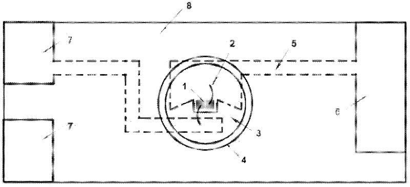
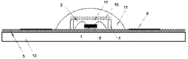
[0026] The white LED is mainly provided with a double-layer substrate with a bracket, a light-emitting chip 1, two connecting wires 2, and a colloid 11. The center of the surface of the white LED is surrounded by a bracket to form a bonding area 3, and a There is a positive electrode 6 and two negative electrodes 7, see figure 2 , the double-layer substrate is mainly provided with an insulating substrate 12 (wherein the insulating substrate 12 is a printed circuit board or a ceramic substrate), the top of the insulating substrate 12 is combined with a conductive layer, and the conductive layer is etched to obtain a conductive pattern 5, and a layer is coated on the top. The isolation glue 8 made of a layer of PU must reserve several parts when coating the isolation glue 8, such as the bonding area 3, the positive electrode 6 and the negative electrode 7 do not need to apply the isolation glue 8.
[0027] The light-emitting chip 1 is bonded to the bonding area 3 of the substra...
PUM
 Abstract
Description
Claims
Application Information