Phosphor layer structure, method for forming same, and light-emitting diode packaging structure

A technology of light-emitting diodes and fluorescent layers, which is applied in transportation and packaging, thin material processing, semiconductor devices, etc. It can solve the problems of poor light output efficiency of light-emitting diodes, inability to effectively control the degree of light mixing, and poor light mixing effects, etc., to achieve mixed light. The effect of better light effect and better light output efficiency

Active Publication Date: 2011-12-07
XUYU OPTOELECTRONICSSHENZHEN CO LTD
View PDF6 Cites 2 Cited by
  • Summary
  • Abstract
  • Description
  • Claims
  • Application Information

AI Technical Summary

Problems solved by technology

However, directly mixing red and green phosphors into the encapsulation colloid cannot effectively control the degree of light mixing, resulting in poor light output efficiency and poor light mixing effect of LEDs.

Method used


Image

  • Phosphor layer structure, method for forming same, and light-emitting diode packaging structure
  • Phosphor layer structure, method for forming same, and light-emitting diode packaging structure
  • Phosphor layer structure, method for forming same, and light-emitting diode packaging structure

Examples


Embodiment approach 1

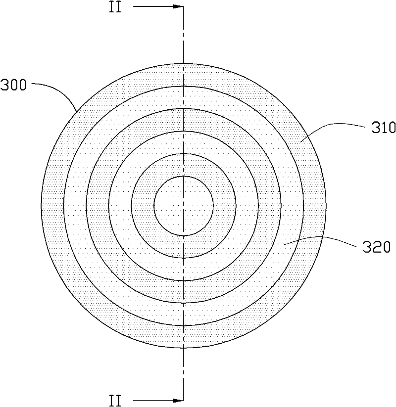
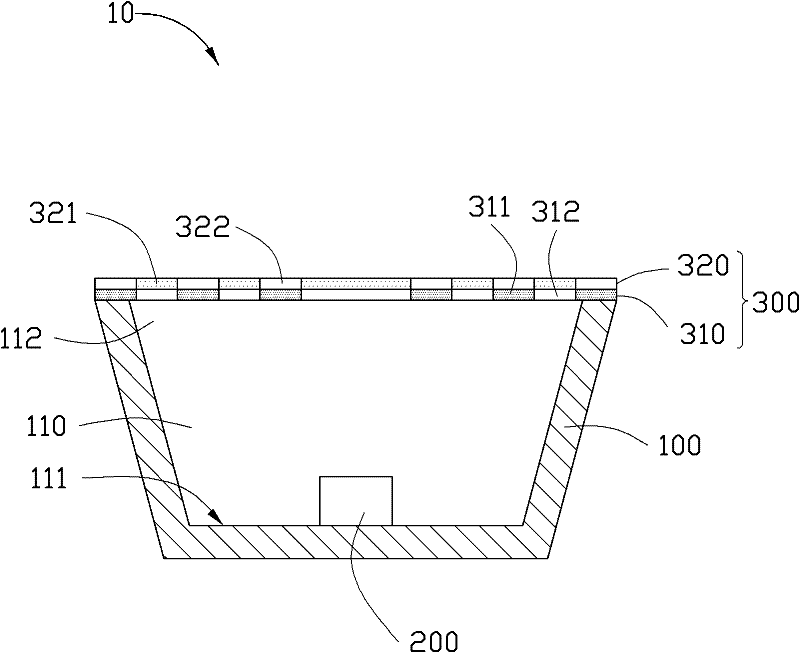
[0045] see figure 1 as well as figure 2 , a light emitting diode packaging structure 10 , which includes an accommodating cup 100 , a light emitting diode chip 200 disposed in the accommodating cup 100 , and a fluorescent layer structure 300 covering the light emitting diode chip 200 .

[0046] The accommodating cup 100 includes an accommodating groove 110 , and the accommodating groove 110 includes a bottom surface 111 and a top opening 112 .

[0047] The LED chip 200 is disposed on the bottom surface 111 of the accommodating groove 110 , and the light emitted by it is emitted from the top opening 112 of the accommodating groove 110 . In this embodiment, the LED chip 200 is a blue light emitting die.

[0048] The fluorescent layer structure 300 includes a first fluorescent layer 310 and a second fluorescent layer 320 stacked on top of each other. The first phosphor layer 310 includes a plurality of concentric first annular phosphor strips 311 spaced apart from each other,...

Embodiment approach 2

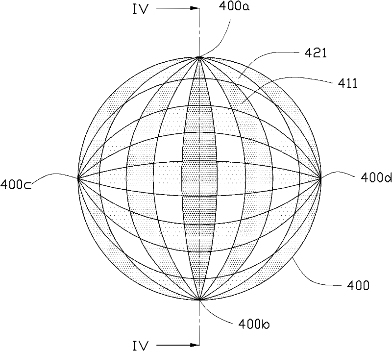
[0052] see image 3 as well as Figure 4 The difference between the LED packaging structure 20 provided in the second embodiment of the present invention and the LED packaging structure 10 in the first embodiment lies in the structure of the fluorescent layer.

[0053] In the second embodiment of the present invention, the fluorescent layer structure 400 is in the shape of a hemispherical shell, which includes a first fluorescent layer 410 and a second fluorescent layer 420 stacked on top of each other. The circular base of the fluorescent layer structure 400 includes a first point 400a, a second point 400b, a third point 400c, and a fourth point 400d, which are located on the plane where the circular base of the fluorescent layer structure 400 is located. The line connecting the first point 400a and the second point 400b is perpendicular to the line connecting the third point 400c and the fourth point 400d. Extending from the first point 400a to the second point 400b, a plu...

Embodiment approach 3

[0057] see Figure 5 as well as Figure 6 The difference between the LED packaging structure 30 provided in the third embodiment of the present invention and the LED packaging structure 10 in the first embodiment lies in the structure of the fluorescent layer.

[0058] In the third embodiment of the present invention, the fluorescent layer structure 500 includes a first fluorescent layer 510 and a second fluorescent layer 520 stacked on each other. The first phosphor layer 510 includes a plurality of first strip-shaped phosphor strips 511 arranged parallel to each other at intervals, and the second phosphor layer 520 includes a plurality of second strip-shaped phosphor strips 521 arranged in parallel at intervals. When the first fluorescent layer 510 and the second fluorescent layer 520 are stacked, the plurality of first strip-shaped phosphor strips 511 and the plurality of second strip-shaped phosphor strips 521 are intersected to form a grid shape. The maximum distance b...


PUM


Abstract

The invention provides a fluorescent layer structure comprising a first fluorescent layer and a second fluorescent layer which are stacked, wherein the first fluorescent layer comprises a plurality of first phosphor powder strips which are spaced from one another, the second fluorescent layer comprises a plurality of second phosphor powder strips which are spaced from one another, and the maximum distance between two adjacent first phosphor powder strips and the maximum distance between two adjacent second phosphor powder strips are both less than 1 mm. Compared with the prior art, in the fluorescent layer structure provided by the invention, the phosphor powder strips are spaced to achieve the purpose of controlling the uniformity of phosphor powders in the fluorescent layer structure, so as to ensure more uniform mixing of light from a light emitting diode and better light output efficiency. The invention also provides a forming method of the fluorescent layer structure and a light emitting diode package structure having the fluorescent layer structure.

Description

technical field [0001] The invention relates to a fluorescent layer structure, a forming method thereof, and a light emitting diode packaging structure. Background technique [0002] Light-emitting diodes are widely used in various light sources due to their small size and the ability to emit bright-colored light with good efficiency. In order to make light-emitting diodes emit light of different colors, the current general practice is to mix phosphors of various colors into the encapsulation colloid to form a fluorescent layer, and then coat it on the light-emitting chip, and use the light emitted by the light-emitting chip to excite the phosphors in the fluorescent layer. phosphors to produce the desired color of light. For example, a yellow phosphor is formed on a blue light-emitting diode, and white light is formed by mixing yellow and blue light beams. Similarly, red and green phosphors can also be used to mix light with blue light-emitting diodes, and this way can ac...

Claims


Application Information

Patent Timeline
Patent Type & Authority Applications(China)
IPC IPC(8): H01L33/50H01L33/48
CPCH01L33/507H01L33/508H01L33/504Y10T428/216Y10T428/24058Y10T428/24868
Inventor 廖启维曾文良林志勇谢明村叶进连
Owner XUYU OPTOELECTRONICSSHENZHEN CO LTD
Why Eureka
Try Eureka