Wafer-level vacuum packaging method for MEMS devices

A technology of vacuum packaging and device wafers, which is applied in the direction of microstructure devices, manufacturing microstructure devices, decorative arts, etc., can solve the problems of changing the performance of anti-reflection coatings or getters, etc., to reduce infrared transmittance and reduce failure rate, the effect of ensuring flatness

Active Publication Date: 2011-12-14
北方广微科技有限公司
View PDF5 Cites 26 Cited by
  • Summary
  • Abstract
  • Description
  • Claims
  • Application Information

AI Technical Summary

Problems solved by technology

However, high temperature, acid, alkali, plasma, etc. may change the performance of the anti-

Method used


Image

  • Wafer-level vacuum packaging method for MEMS devices
  • Wafer-level vacuum packaging method for MEMS devices
  • Wafer-level vacuum packaging method for MEMS devices

Examples


Embodiment Construction

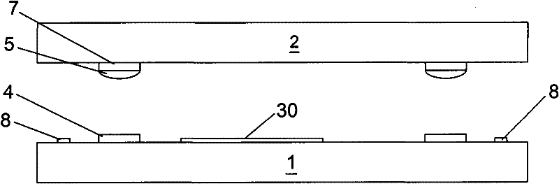
[0060] The wafer-level vacuum packaging method for micro-electromechanical devices will be described below by taking the packaging of an uncooled infrared microbolometer chip as an example.

[0061] refer to Figure 3A-Figure 3H , Figure 4 and Figure 5 . According to the method of the present invention, the wafer-level vacuum packaging method of the uncooled infrared microbolometer chip 30 includes the following steps in sequence:

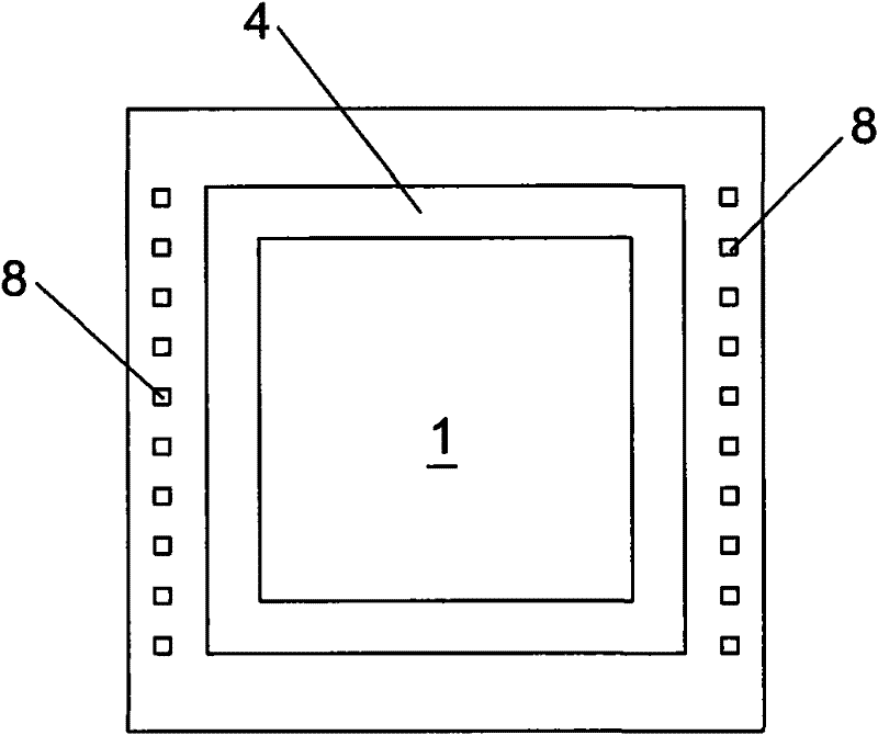
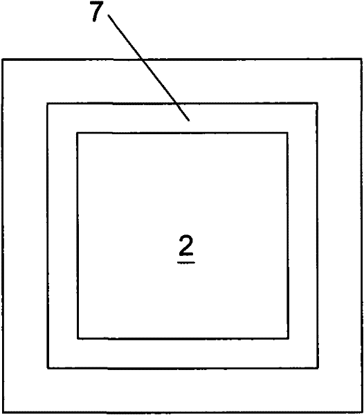
[0062] S1. Wafer preparation: prepare capping wafer 2 and device wafer 1 . An uncooled infrared microbolometer 30 and a lead plate 8 have been prepared in the device wafer 1 . figure 2 As shown, the capping wafer used in the wafer-level vacuum packaging method of micro-electromechanical devices of the present invention is silicon-insulating material, and the silicon-insulating material includes a front silicon layer 2a, a silicon dioxide intermediate layer 2b and a reverse silicon layer 2c, Among them, the silicon layer on the back side is ...


PUM

PropertyMeasurementUnit
Thicknessaaaaaaaaaa

Abstract

The invention provides a wafer-level vacuum encapsulating method for a micro-electromechanical device, which sequentially comprises the following steps of: 1, preparing a capping wafer and a device wafer, wherein the capping wafer is insulated silicon consisting of a front silicon layer, a back silicon layer and a middle silicon dioxide layer; 2, growing sealing rings on the front of the device wafer and the front of the capping wafer; 3, growing solder on the sealing ring on the front of the capping wafer; 4, performing deep silicon etching on the capping wafer by taking the sealing ring as a mask to obtain a groove; 5, growing a getter film on the front of the capping wafer, wherein the pattern of the getter film is obtained by a maskplate during growth; 6, heating to activate the getter film and bonding the capping wafer and the device wafer together by using bonding equipment; 7, growing an antireflection film on the back of the capping wafer, wherein the pattern of the antireflection film is obtained by the maskplate during growth; and 8, cutting the wafers. By adjusting process order, the influence of a next process on a result of a previous process is avoided, and the method is particularly suitable for encapsulating infrared devices.

Description

technical field [0001] The invention relates to a wafer-level vacuum packaging method for a micro-electromechanical device. Background technique [0002] For micro-electromechanical (MEMS) devices, the traditional packaging technology is mainly chip-level packaging. The process flow includes the following steps: firstly prepare the MEMS chip on the silicon wafer; then slice the wafer, release the sacrificial layer, patch, lead wire; finally seal the cap. Among these steps, the steps after releasing the sacrificial layer are all performed on a single chip. Since a wafer can be diced to produce hundreds of chips, the cost of such chip-scale packaging is high. In fact, about 90% of the cost of a finished MEMS device is spent on packaging. Therefore, reducing packaging costs is a major development trend of the MEMS industry. Integrated circuits (ICs) have achieved wafer-level packaging. On the basis of referring to the wafer-level packaging technology of integrated circuits,...

Claims


Application Information

Patent Timeline
IPC IPC(8): B81C1/00
Inventor 方辉郭俊雷述宇
Owner 北方广微科技有限公司
Why Eureka
Try Eureka