

Image sensor pixel unit and clamping circuit
A technology of image sensor and pixel unit, which is applied in TV, electrical components, image communication, etc., and can solve the problems of being unsuitable for high-density CMOS image sensors and occupying chip area.
- Summary
- Abstract
- Description
- Claims
- Application Information
AI Technical Summary
Problems solved by technology
Method used
Image

Examples
Embodiment Construction
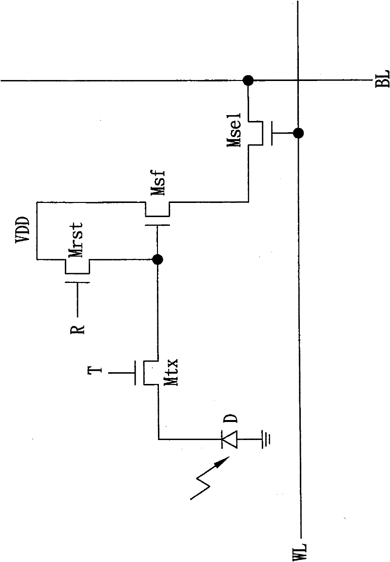
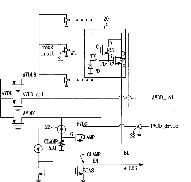
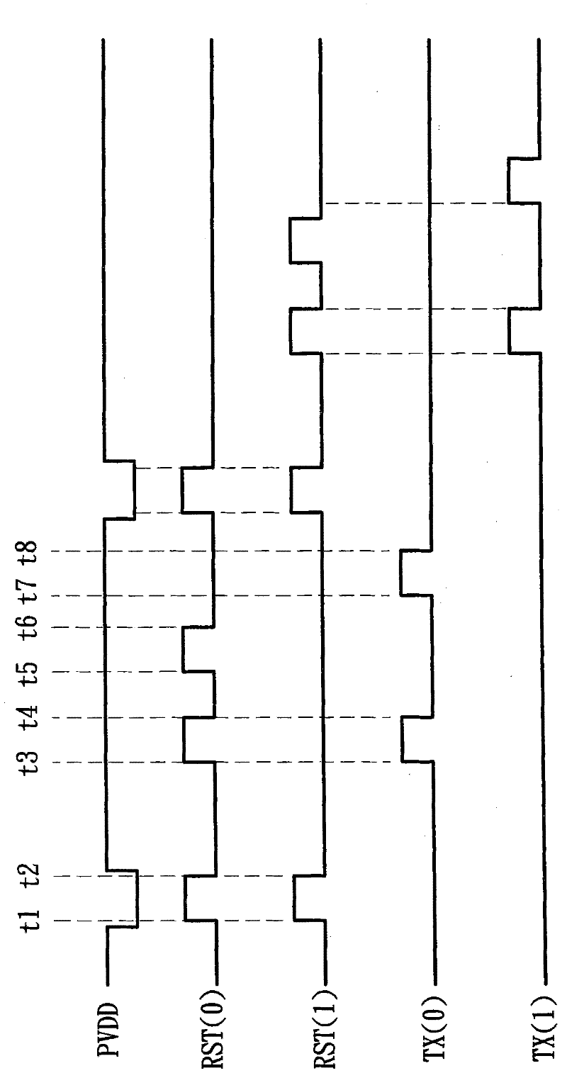
[0012] Figure 2A A complementary metal oxide semiconductor (CMOS) image sensor according to a first embodiment of the present invention is shown. For ease of description, only the main circuit structures related to the embodiments of the present invention are shown.
[0013] In this embodiment, each pixel unit 20 includes a photodetector (such as a photodiode) PD, a transfer gate TX, a reset transistor RST and a source follower SF. Compared with the traditional four-transistor (4T) pixel unit, this embodiment omits the selection transistor, thus increasing the light-sensing area, but still has the function of the traditional 4T pixel unit. Wherein, the drain D of the reset transistor (for example, N-type MOS transistor) RST is electrically connected to the drain D of the source follower (for example, N-type MOS transistor) SF; the source S of the reset transistor RST is electrically connected to the source The gate of the pole follower SF (that is, the floating diffusion re...
PUM
 Abstract
Description
Claims
Application Information