
Etching apparatus, analysis apparatus, etching treatment method, and etching treatment program

A technology of etching processing and etching equipment, which is applied in the directions of electrical excitation analysis, thermal excitation analysis, material excitation analysis, etc., and can solve the problems of unable to find waveforms, unable to classify waveforms, and unable to evaluate

Active Publication Date: 2013-10-23
HITACHI HIGH-TECH CORP
View PDF7 Cites 0 Cited by
  • Summary
  • Abstract
  • Description
  • Claims
  • Application Information

AI Technical Summary

Problems solved by technology

[0020] However, in the method described in Patent Document 1, although the emission wavelength can be limited based on the peak of the emission originating from the same substance, it is not possible to classify the emission at wavelengths other than the setting information of the spectral line corresponding to the substance.
In addition, regarding the waveform, there is no description of the method of evaluating the commonality of the change, and the classification of the wavelength based on the reaction cannot be realized.
[0021] In addition, in the method described in Patent Document 2, although it is possible to evaluate changes in luminous intensity (corresponding to waveforms) in all wavelength regions that change in common by evaluating the main components obtained by the main component analysis, it cannot Partial differences in waveforms are evaluated to classify wavelength
[0022] Also, in the method described in Patent Document 3, similarly to the method described in Patent Document 2, wavelengths cannot be classified.
[0023] In addition, in the method described in Patent Document 4, only a technique for extracting wavelengths of waveforms with large variations by principal component analysis is described, and a technique for classifying a plurality of waveforms is not disclosed.
[0024] In addition, in the method described in Patent Document 5, it is necessary to register patterns in advance in the classification of changing patterns, so it is impossible to classify waveforms that vary in various ways depending on the content of the etching process.
[0025] In addition, in the method described in Patent Document 6, the time change of the luminous intensity of plasma luminescence is analyzed, and the luminous intensity level at the time before the end point of the plasma treatment and the luminous intensity level at the time after the end point are analyzed. However, it is only possible to evaluate waveform changes based on two intensity differences, so it is not possible to adequately classify waveforms that vary in various ways.
[0026] In addition, in the method described in Patent Document 7, a correlation between emission wavelengths is generated, and the end point of the etching process is detected from the angle between the principal component vectors of the relevant principal components. However, even if the angle between the vectors is checked, only common changes at multiple wavelengths can be found, and it is impossible to find representative wavelengths from waveforms that vary in various ways.

Method used


Image

  • Etching apparatus, analysis apparatus, etching treatment method, and etching treatment program
  • Etching apparatus, analysis apparatus, etching treatment method, and etching treatment program
  • Etching apparatus, analysis apparatus, etching treatment method, and etching treatment program

Examples


Embodiment Construction

[0059] Hereinafter, embodiments of the present invention will be described in detail with reference to the drawings. In addition, in all the drawings for describing the embodiments, the same members are given the same reference numerals in principle, and repeated description thereof will be omitted.

[0060] First, the outline of the present invention will be described.

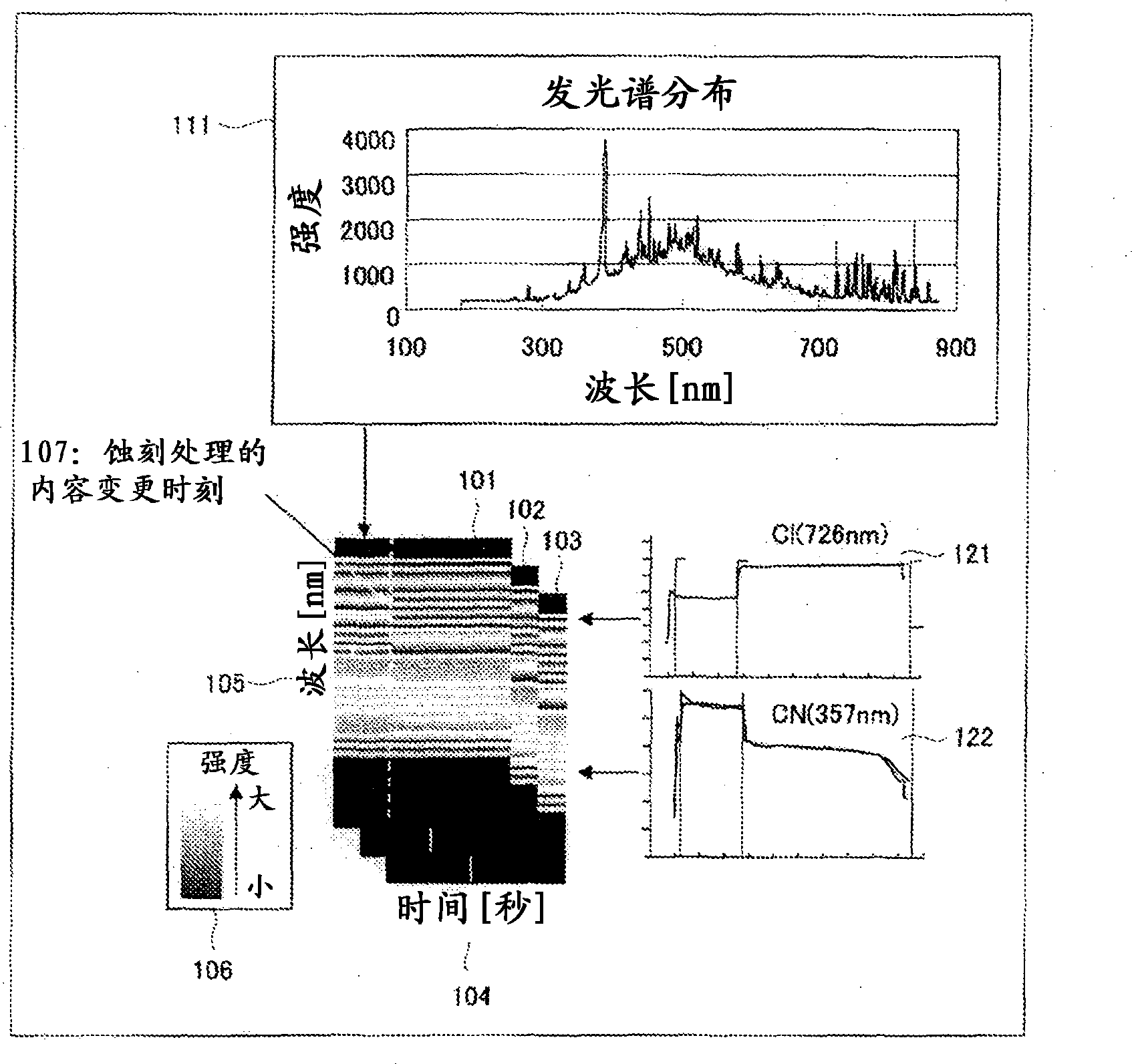
[0061] In the present invention, the etching apparatus is equipped with an optical splitter (OES), and includes means for acquiring OES data for each etching process. The light-emitting spectrometer is connected to a storage device and a database, and includes means for storing OES data in the storage device and the database. Equipped with: a unit that obtains multiple waveforms from OES data, classifies the waveforms, and obtains representative waveforms to monitor etching; a unit that judges abnormality / normality; a unit that analyzes / evaluates etching processing results; and a unit that adjusts etching pr...


PUM


Abstract

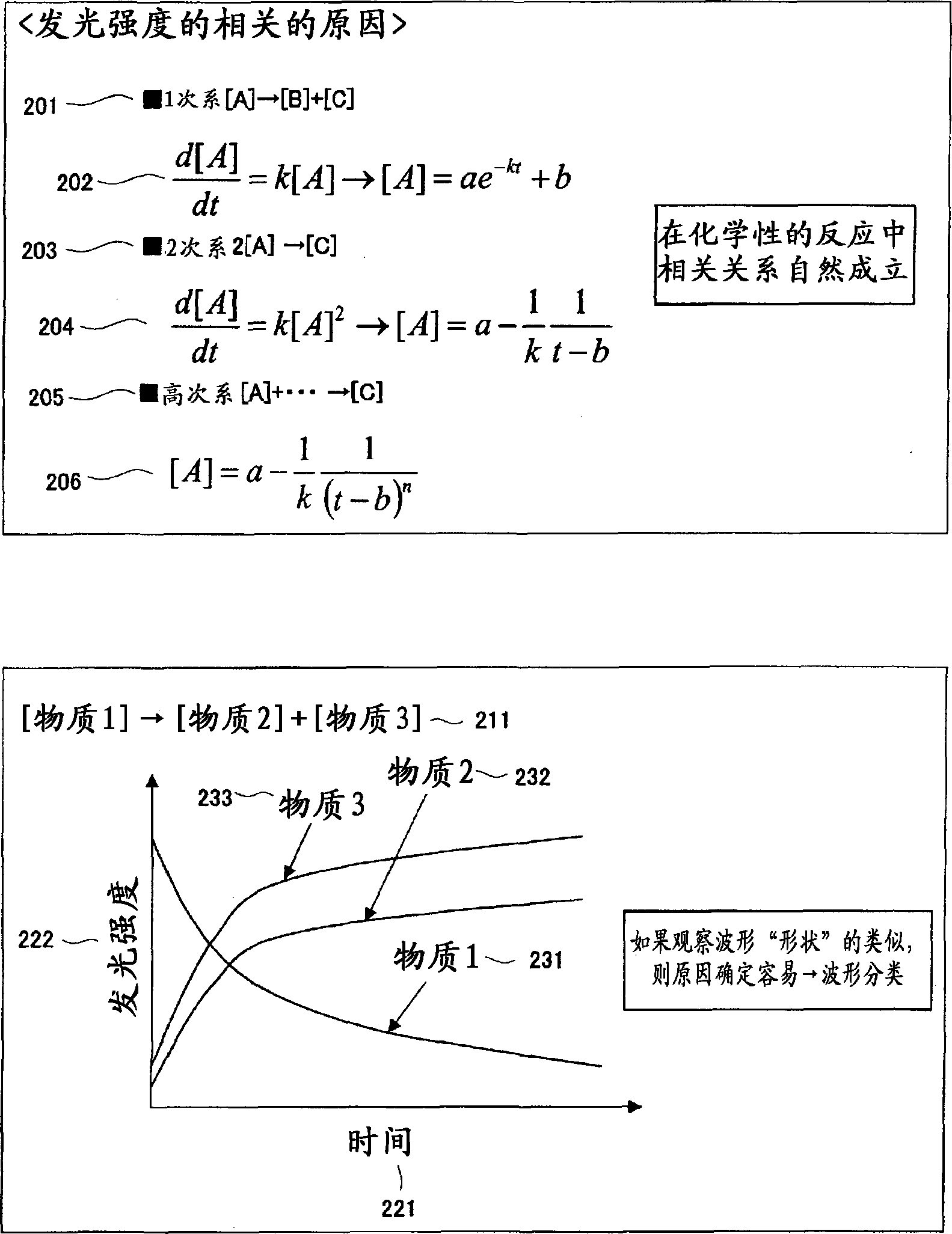
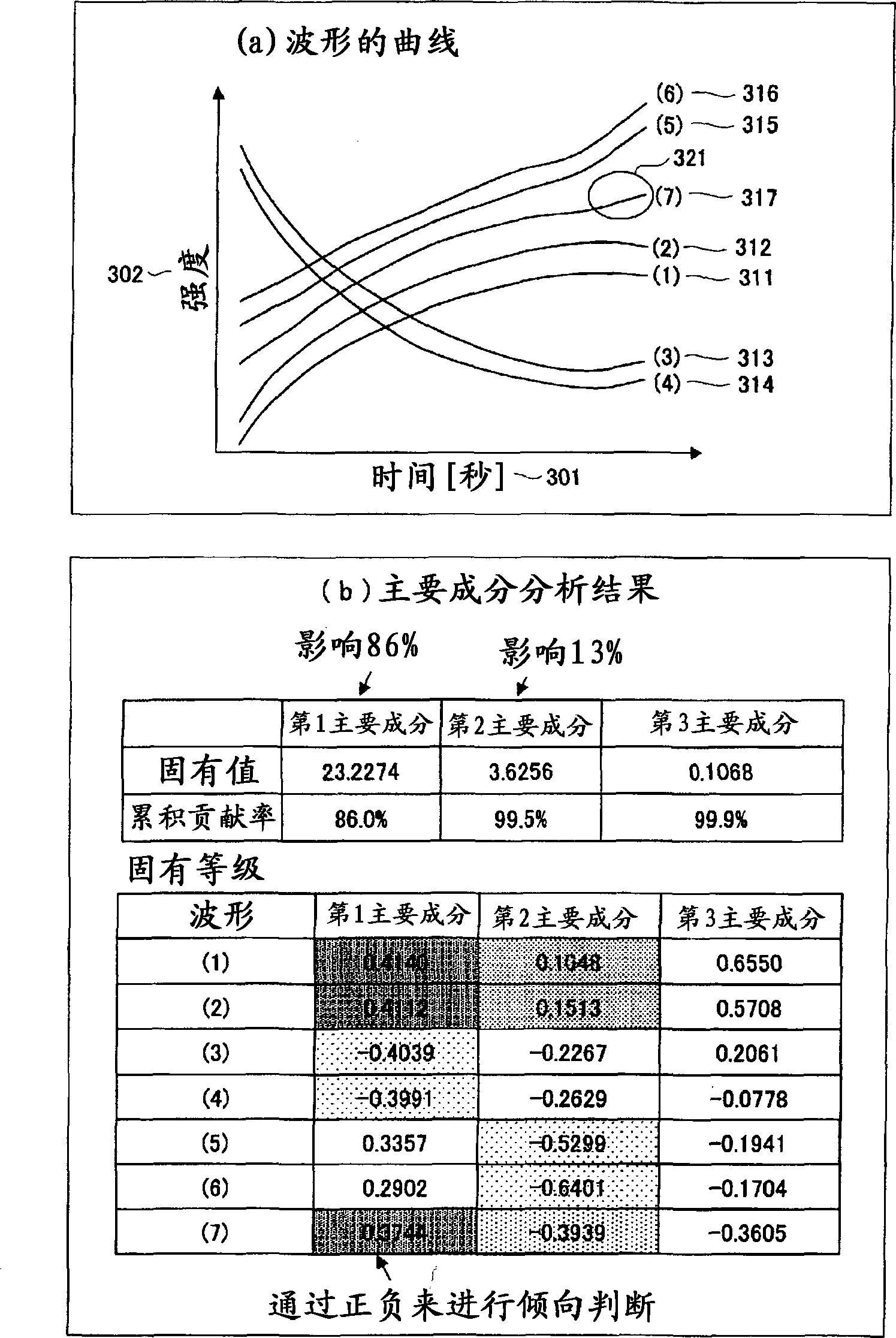
There is provided an etching apparatus in which, without setting the information of the substance and the chemical reaction, a small number of representative wavelengths can be selected from a waveform at a lot of wavelengths, and an analysis process of etching data which needs large man-hours can be eliminated to efficiently set the monitoring of the etching. The etching apparatus includes: a lot / wafer / step-depending OES-data searching / acquiring function 511 for acquiring a plurality of optical emission intensity waveforms along an etching-treatment time axis; a waveform-change-existence judgment function 521 for judging the existence of the change of the plurality of light emission intensity waveforms; a waveform-correlation-matrix calculating function 522 for calculating a correlation matrix between the optical emission intensity waveforms; a waveform classifying function 523 for classifying the optical emission intensity waveforms into groups; and a representative-waveform selecting function 524 for selecting a representative optical emission intensity waveform from the group.

Description

technical field [0001] The present invention relates to a method of classifying waveforms of luminescence intensity during etching processing in an etching device and an analysis device for monitoring plasma emission in the etching device, and selecting a waveform that affects the etching processing result. In particular, it relates to a method of classifying wavelengths based on the similarity of waveform "shape" to select a representative wavelength, or a method of quantitatively determining a waveform with little variation. Background technique [0002] In order to obtain a fine shape such as a semiconductor device formed on a wafer, an etching process is performed in which a substance is ionized by plasma and the substance acts on the substance (reaction on the wafer surface) to remove the substance on the wafer. There are various ionized substances, and the substances on the wafer also vary according to product functions. [0003] Furthermore, in order to form a shape ...

Claims


Application Information

Patent Timeline
Patent Type & Authority Patents(China)
IPC IPC(8): H01L21/3065G01N21/66G01N21/71H05H1/00
CPCH01J37/32972H05H1/0037G01N21/68H01J37/32935H01L21/3065G01N21/66G01N21/71
Inventor 森泽利浩白石大辅井上智己
Owner HITACHI HIGH-TECH CORP
Learn More