A bonding method for micro-optical components

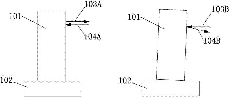
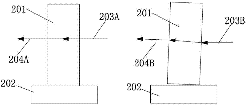
A bonding method and micro-optical technology, applied in optical components, optics, installation, etc., can solve problems such as inconsistent expansion coefficient, uneven thickness of glue layer or solder layer, and angle of incident light 203B, etc., and achieve good temperature stability sexual effect

Inactive Publication Date: 2011-12-21
SHANGHAI BRANCH FUZHOU GAOYI COMM CO LTD
View PDF1 Cites 2 Cited by
  • Summary
  • Abstract
  • Description
  • Claims
  • Application Information

AI Technical Summary

Problems solved by technology

like figure 1 , the micro-optical element 101 is a mirror, and the connection element 102 is connected together with glue or solder. We hope to get such figure 1 In the case on the left side of the middle, the reflected light 104A is parallel to the incident light 103A, but the reality is that the adhesive layer or the solder layer cannot be pressed very uniformly, and there will be figure 1 The situation on the right side of the center causes the angle between the reflected light 104B and the incident light 103B to appear
like figure 2 For a transmission etalon, we hope to obtain figure 2 In the case of the action, the incident light 203A and the refracted light 204A are parallel, but, and figure 1 In the same situation as the case, if the micro-optical element 201 cannot be in good plane contact with the connecting element 202 to produce a corner of the adhesive layer, then it will appear as figure 2 The situation on the right side of the center causes the angle between the refracted light 204B and the incident light 203B
Since the optical system has relatively high temperature performance requirements, and at the same time, due to the uneven thickness of the adhesive layer or solder layer, its expansion coefficient is inconsistent with that of the bonding component, and it will move uniformly when the temperature changes, thus affecting the temperature performance of the optical component.

Method used


Image

  • A bonding method for micro-optical components
  • A bonding method for micro-optical components
  • A bonding method for micro-optical components

Examples


Embodiment Construction

[0011] The present invention will be further described below in conjunction with the accompanying drawings and specific embodiments.

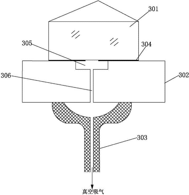
[0012] 301. Micro-optical components, 302. Connecting components, 303 . Exhaust pipe, 304. glue or solder, 305. cavity, 306. air hole.

[0013] Such as image 3 As shown, one or more cavities 305 smaller in size than the micro-optical element 301 are processed at the place where the connection element 302 will be bonded with the micro-optical element 301, and a corresponding air hole 306 is processed at the center of the cavity 305 of the connection element 302 , the cavity 305 and the vent hole 306 can be a combination of one or more pairs of arrays, and the specific bonding process is: apply glue or solder 304 around the position of the connection element 302 to be bonded, that is, the cavity 305, and then Put the micro-optical element 301 on the position where the connecting element 302 is to be bonded, turn on the vacuum pump, and the ai...


PUM


Abstract

The invention discloses a bonding method for a micro-optical element, which is characterized in that a cavity is set in the bonding surface between two closely connected elements to be bonded or welded, especially between the micro-optic element and the connecting piece, and at the same time There is a vent hole, and the vent hole is connected by a vacuum pump. The optical element and the connecting element are in close contact under the action of atmospheric pressure. The adhesive layer or molten solder is evenly distributed and solidified on the contact surface, thereby obtaining better temperature stability.

Description

technical field [0001] The invention relates to the field of optical and optical fiber communication passive devices, in particular to a bonding method for micro-optical components. Background technique [0002] When bonding or soldering micro-optical components and connectors, it is often difficult to apply a uniformly distributed force so that the glue or solder layer is evenly distributed. like figure 1 , the micro-optical element 101 is a mirror, and the connection element 102 is connected together with glue or solder. We hope to get such figure 1 In the case on the left side of the middle, the reflected light 104A is parallel to the incident light 103A, but the reality is that the adhesive layer or the solder layer cannot be pressed very uniformly, and there will be figure 1 In the case on the right side, the angle between the reflected light 104B and the incident light 103B is caused. like figure 2 For a transmission etalon, we hope to obtain figure 2 In the cas...

Claims


Application Information

Patent Timeline
Patent Type & Authority Applications(China)
IPC IPC(8): G02B7/00
Inventor 吴砺凌吉武李阳胡豪成郑保忠
Owner SHANGHAI BRANCH FUZHOU GAOYI COMM CO LTD
Why Eureka
Try Eureka