Stacked chip package structure and method

A chip packaging structure and chip packaging technology, applied in the direction of electrical components, electric solid devices, circuits, etc., can solve the problems of large package structure, high cost, and inability to meet the development trend of miniaturization of electronic products, so as to reduce the volume of products Effect

Active Publication Date: 2011-12-21
SHUNSIN TECH (ZHONG SHAN) LTD
View PDF10 Cites 2 Cited by
  • Summary
  • Abstract
  • Description
  • Claims
  • Application Information

AI Technical Summary

Problems solved by technology

However, this packaging structure has a large volume and cannot meet the development trend of miniaturization of electronic products, and the cost is relatively high

Method used


Image

  • Stacked chip package structure and method
  • Stacked chip package structure and method
  • Stacked chip package structure and method

Examples


Embodiment Construction

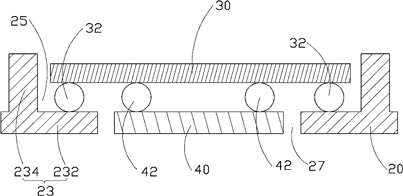
[0027] figure 1 It is a schematic cross-sectional view of the assembly of the stacked chip packaging structure 100 without the encapsulant 10 of the present invention. Please also refer to FIG. 3( e ), the stacked chip packaging structure 100 of the present invention includes an encapsulant 10 , a substrate 20 , a first chip 30 and a second chip 40 .

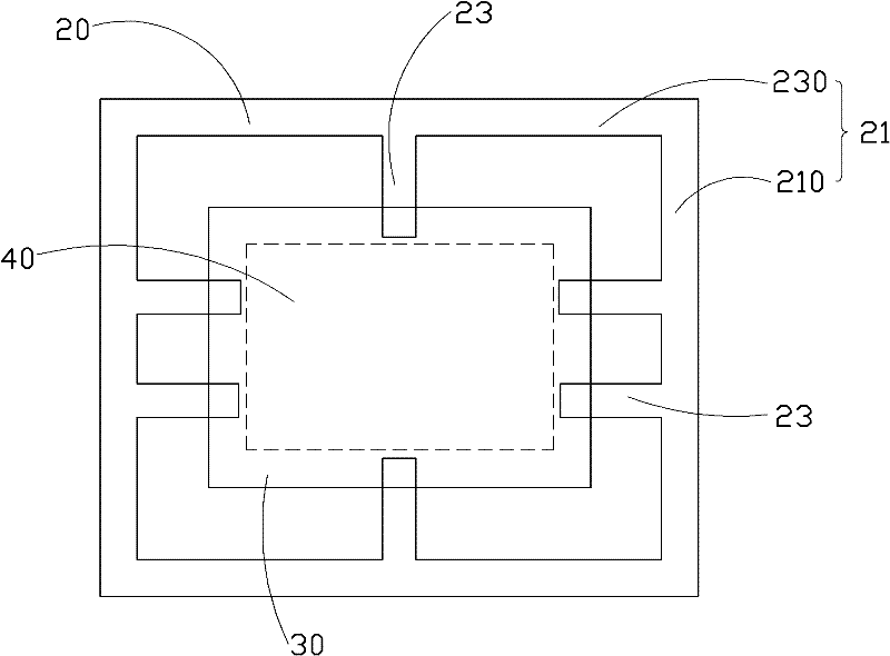
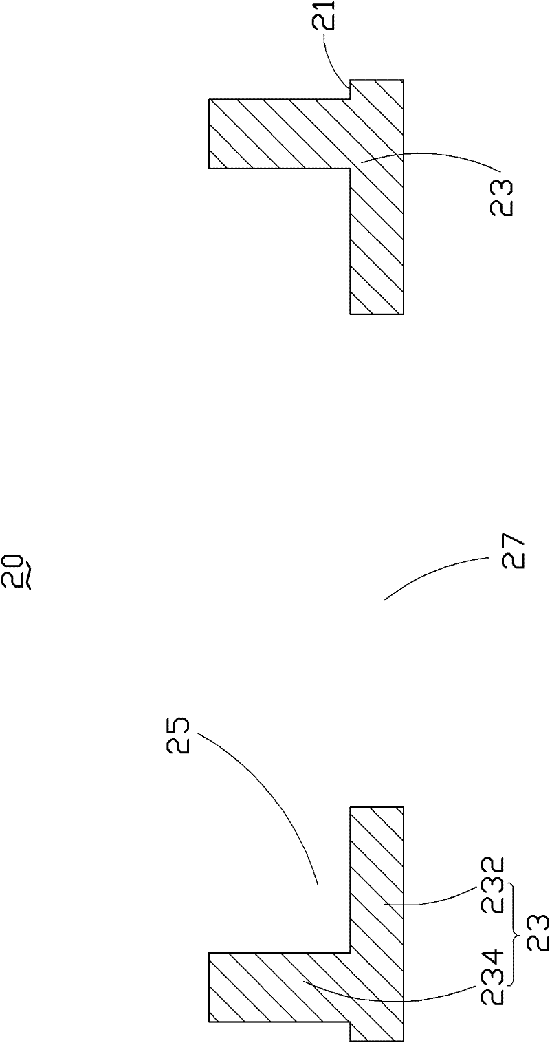
[0028] Please refer to figure 1 and figure 2 , the substrate 20 is a frame structure, which includes a body 21 , a plurality of pins 23 , a receiving portion 27 and a recessed portion 25 . The body 21 includes a pair of opposite first sidewalls 210 and a pair of opposite second sidewalls 230 , and the first sidewalls 210 and the second sidewalls 230 are respectively connected vertically.

[0029] The pins 23 are independent from each other and connected to the body 21 respectively. In this embodiment, there are six pins 23 . Wherein, the inner wall of each first side wall 210 is respectively connected with a pair of pins 2...


PUM


Abstract

The invention relates to a stacking type chip packaging structure, which comprises a substrate, a first chip, a second chip and a packaging rubber body. The substrate comprises a plurality of pins, an accommodating part and a depression part, and the depression part is arranged in the middle area of the substrate and is surrounded by the pins. The accommodating part is arranged under the depression part and is communicated with the depression part. The first chip is fixed on the pins and is hidden in the depression part. The second chip is fixed on the first chip and is accommodated in the accommodating part, and the top surface of the second chip is parallel and level with the bottom surface of the pins. The packaging rubber body is used for packaging the substrate, the first chip and the second chip and is filled in the depression part and the accommodating part. The invention also provides a stacking type chip packaging method. By adopting the stacking type chip packaging structure and the stacking type chip packaging method, the first chip and the second chip are hidden in the substrate, so that the product size is reduced.

Description

technical field [0001] The invention relates to semiconductor packaging technology, in particular to a stacked chip packaging structure and method. Background technique [0002] In the existing stacked chip packaging structure, the first chip is stacked on the top surface of the substrate and the second chip is stacked on the top surface of the first chip. However, this packaging structure has a large volume, cannot meet the development trend of miniaturization of electronic products, and has high cost. Contents of the invention [0003] In view of this, it is necessary to provide a stacked chip packaging structure capable of reducing the volume. [0004] It is also necessary to provide a stacked chip packaging method capable of reducing the volume. [0005] A stacked chip packaging structure, including a substrate, a first chip, a second chip and an encapsulant. The substrate includes a plurality of pins, a receiving portion and a recessed portion, the recessed portion...

Claims


Application Information

Patent Timeline
Patent Type & Authority Applications(China)
IPC IPC(8): H01L25/00H01L23/13H01L21/50H01L21/58
CPCH01L2224/16245
Inventor 肖俊义
Owner SHUNSIN TECH (ZHONG SHAN) LTD
Why Eureka
Try Eureka