Light-emitting diode with current blocking layer and manufacturing method thereof

A technology of light-emitting diodes and current blocking, applied in circuits, electrical components, semiconductor devices, etc., can solve the problems of high cost, unsatisfactory density and hardness of the oxide insulating layer, and inability to completely block current transport, etc. Achieve the effect of good current blocking effect and low cost

Inactive Publication Date: 2011-12-21
冠铨(山东)光电科技有限公司
View PDF6 Cites 5 Cited by
  • Summary
  • Abstract
  • Description
  • Claims
  • Application Information

AI Technical Summary

Problems solved by technology

However, the oxide insulating layer deposited by this method is generally not very ideal in terms of density and hardness.
In addition, there is another method for making a current blocking layer, which is to form a current blocking layer directly below the electrode in the p-type semiconductor epitaxial layer by ion implantation or diffusion. The thickness and structure of the current blocking layer formed by this method are difficult. Precise control leads to the expansion of current under the electrode, which cannot completely block the transport of current under the electrode, and the ion implantation and diffusion process is complicated and the cost is high

Method used


Image

  • Light-emitting diode with current blocking layer and manufacturing method thereof
  • Light-emitting diode with current blocking layer and manufacturing method thereof
  • Light-emitting diode with current blocking layer and manufacturing method thereof

Examples


Embodiment Construction

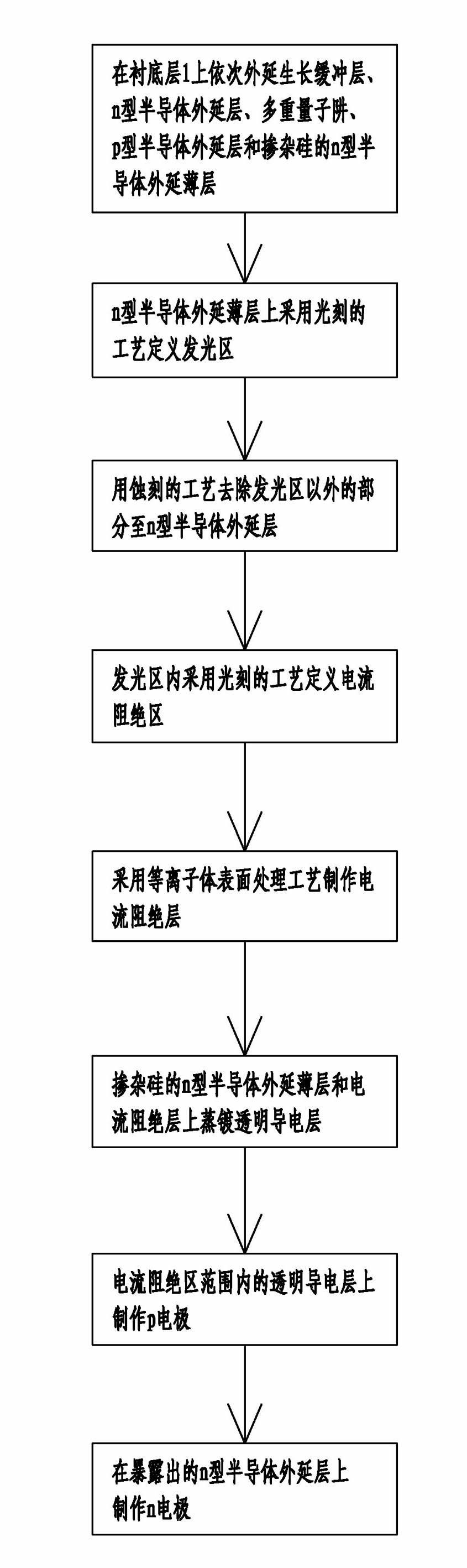
[0027] For ease of description, the light-emitting diode provided with a current blocking layer and its manufacturing method of the present invention will be described in detail below in conjunction with the accompanying drawings:

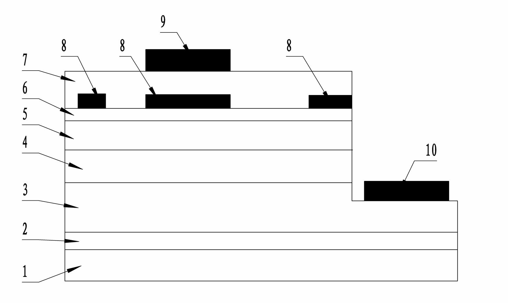
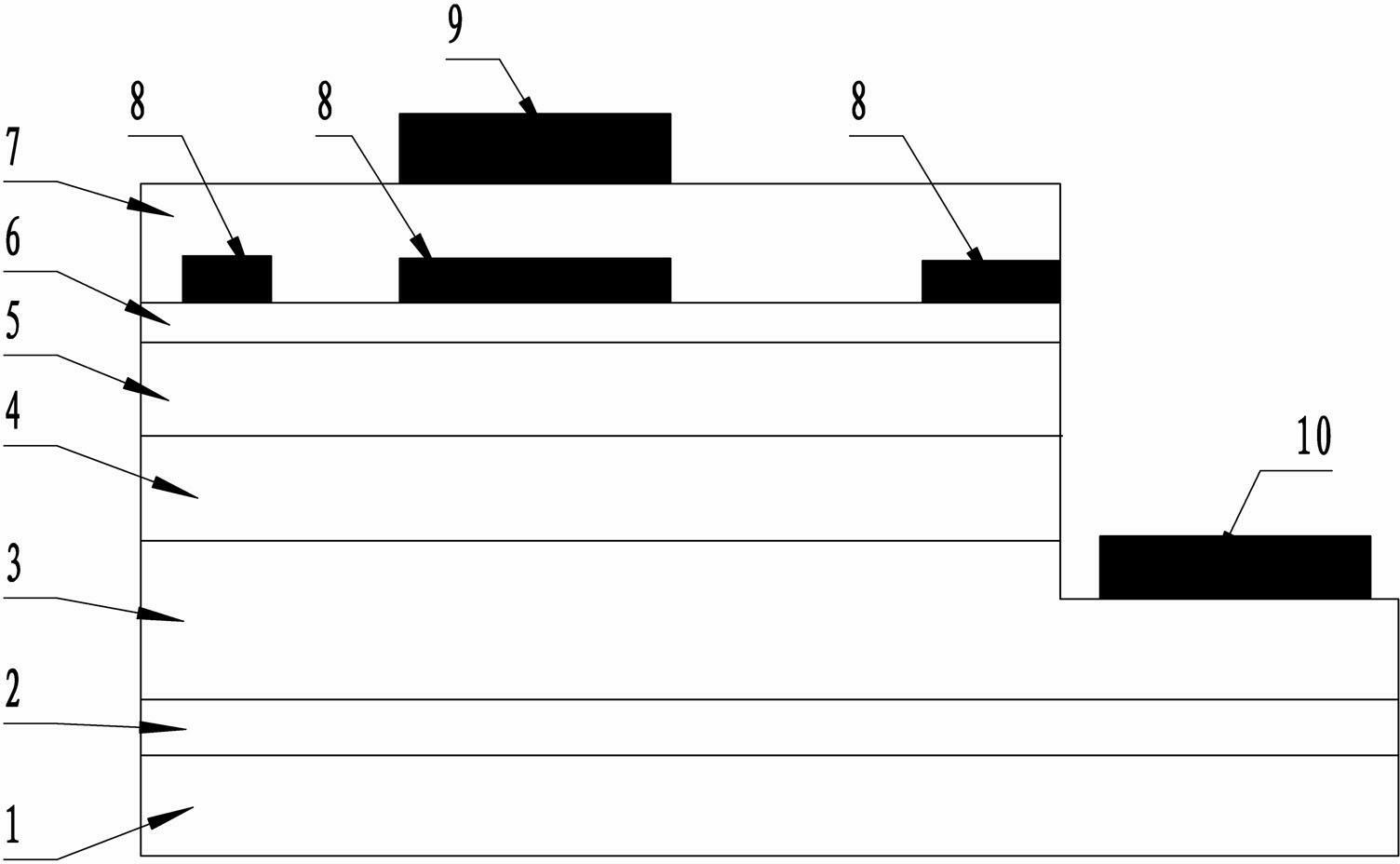
[0028] As attached figure 1 As shown in, a light-emitting diode provided with a current blocking layer includes a substrate layer 1, a buffer layer 2, an n-type semiconductor epitaxial layer 3, a multiple quantum well 4, and a p-type semiconductor epitaxial layer 5 arranged from bottom to top. The p-type semiconductor epitaxial layer 5 is further provided with a silicon-doped n-type semiconductor epitaxial thin layer 6, and the silicon-doped n-type semiconductor epitaxial thin layer 6 is provided with a current blocking layer 8 in the defined light-emitting area , The silicon-doped n-type semiconductor epitaxial thin layer 6 and the current blocking layer 8 are provided with a transparent conductive layer 7, and the transparent conductive la...


PUM


Abstract

The invention provides a light-emitting diode with a current blocking layer, comprising an n-type semiconductor epitaxial layer, a multiple quantum well, and a p-type semiconductor epitaxial layer arranged in sequence from bottom to top, and the p-type semiconductor epitaxial layer is further provided with A silicon-doped n-type semiconductor epitaxial thin layer, a current blocking layer is arranged in the light-emitting region defined on the silicon-doped n-type semiconductor epitaxial thin layer, and the silicon-doped n-type semiconductor epitaxial thin layer and The current blocking layer is provided with a transparent conductive layer, the transparent conductive layer is provided with a p-electrode, the p-electrode is arranged above the range of the current blocking layer, and the n-type semiconductor epitaxial layer is provided with an n-electrode ; According to the above light-emitting diodes, the present invention provides its manufacturing method. The light-emitting diode provided with the current blocking layer of the present invention has the advantages of ideal compactness and hardness of the current blocking layer, simple manufacturing process and low cost.

Description

technical field [0001] The invention relates to the field of semiconductors, in particular to a light emitting diode, in particular to a light emitting diode provided with a current blocking layer and a manufacturing method thereof. Background technique [0002] As a new type of lighting element, light-emitting diodes have been widely used because of their advantages of high brightness and light efficiency. The chip structure of a traditional light-emitting diode generally includes a substrate layer, a buffer layer, an n-type semiconductor epitaxial layer, a multiple quantum well, a p-type semiconductor epitaxial layer, and a transparent conductive layer from bottom to top. There are metal n-electrode and p-electrode, and the p-electrode is set on the light-emitting area and occupies a certain area. In the arrangement of the p-electrode and the transparent conductive layer, most of the current will gather directly below the electrode, which cannot be well Lateral transporta...

Claims


Application Information

Patent Timeline
IPC IPC(8): H01L33/14H01L33/00
Inventor 吴哲雄刘艳张峻嘉颜廷丽
Owner 冠铨(山东)光电科技有限公司
Why Eureka
Try Eureka