
LED structure and manufacturing method thereof

A technology of LED structure and manufacturing method, applied in electrical components, circuits, semiconductor devices, etc., can solve the problems of high manufacturing cost and insufficient luminous brightness, and achieve the effects of reducing dosage, good current blocking effect, and high industrial practical value.

Pending Publication Date: 2022-01-11
TIANJIN SANAN OPTOELECTRONICS
View PDF0 Cites 0 Cited by
  • Summary
  • Abstract
  • Description
  • Claims
  • Application Information

AI Technical Summary

Problems solved by technology

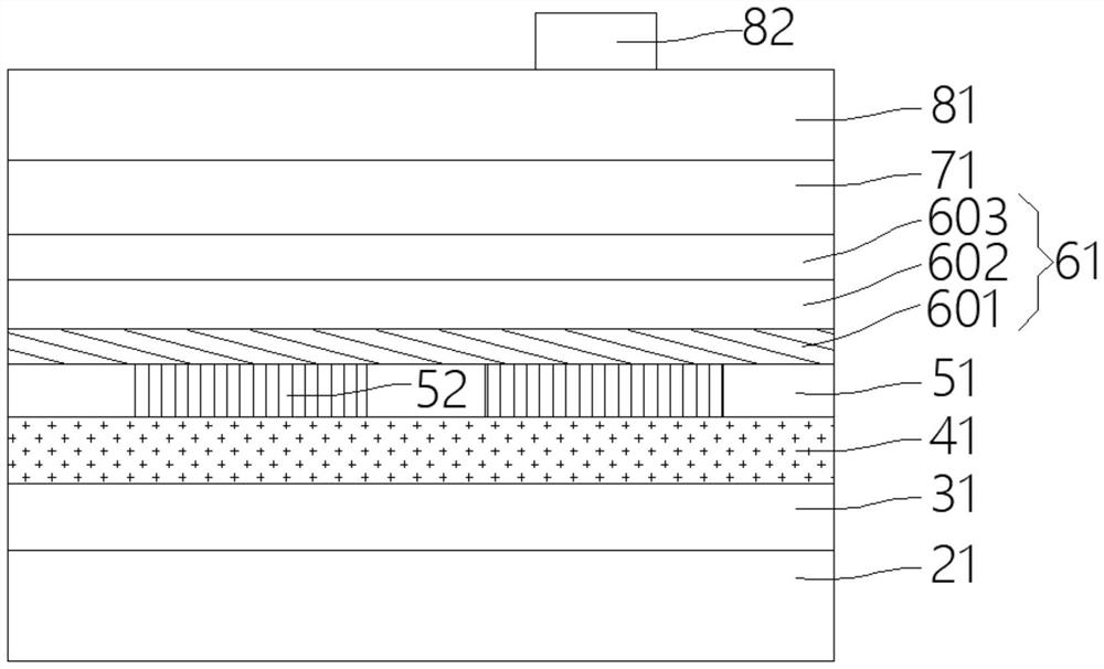
[0005] In view of the above-mentioned shortcomings of the prior art, the purpose of the present invention is to provide an LED structure and manufacturing method, which are used to solve the problems of high manufacturing cost, existence of bonding gaps, and insufficient luminous brightness in the prior art.

Method used


Image

  • LED structure and manufacturing method thereof
  • LED structure and manufacturing method thereof
  • LED structure and manufacturing method thereof

Examples


Embodiment 2

[0093] This embodiment provides a method for manufacturing an LED structure, the method comprising:

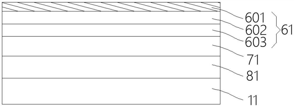
[0094] S1: Provide a semiconductor structure, which includes a substrate layer 11, a first conductivity type semiconductor layer 81, an active layer 71, and a second conductivity type semiconductor layer 61 stacked in sequence, and the second conductivity type semiconductor layer includes a current Extension layer 601, such as image 3 shown;

[0095] Specifically, the substrate layer 11 is an epitaxial substrate, which may be a sapphire substrate, a Si substrate or a SiC substrate. The semiconductor structure may be a material system such as GaN, GaP, AlGaInP, etc., which is not limited here. The second conductivity type semiconductor layer 61 includes a current spreading layer 601 , the current spreading layer 601 may be p-type GaP, and the current spreading layer 601 may further include a transition layer 602 and a barrier layer 603 .

[0096] S2: patterning the current ...


PUM

PropertyMeasurementUnit
thicknessaaaaaaaaaa
diameteraaaaaaaaaa

Abstract

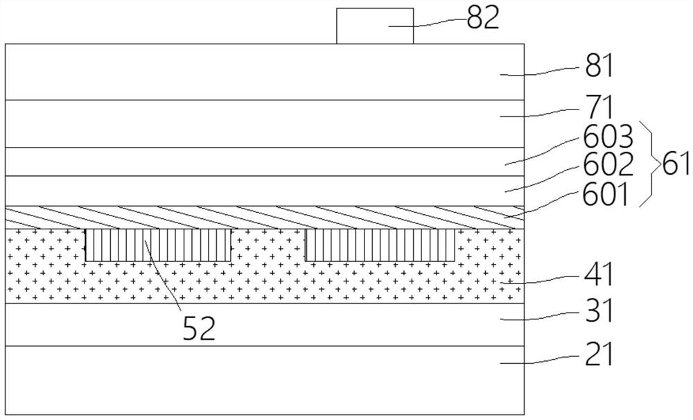
The invention provides an LED structure and a manufacturing method thereof. The LED structure comprises a first conductive type semiconductor layer, an active layer, a second conductive type semiconductor layer, an insulating layer, a contact layer and other functional layers. According to the LED structure, the insulating layer is arranged in the current expansion layer of the second conductive type semiconductor layer, so that light absorption of the second conductive type semiconductor layer can be reduced, the insulating layer is closer to the active layer, a better current blocking effect can be achieved, current is limited in an effective light emitting area, and meanwhile, the height difference between the insulating layer and the surface of the current expansion layer is reduced, so that the consumption of filling metal is reduced when the contact layer is formed, and the manufacturing cost is reduced. In addition, the surface of the contact layer is flush with the surface of the insulating layer, a flat interface can be formed, subsequent bonding gaps are avoided, and the reliability of the LED is improved. Therefore, the LED structure has high industrial practical value.

Description

technical field [0001] The invention relates to the field of semiconductor devices, in particular to an LED structure and a manufacturing method. Background technique [0002] LED is a light-emitting diode, and its essential structure is a semiconductor pn junction, which can directly convert electrical energy into light energy. In the vertical LED structure, it is usually necessary to set an insulating layer (also known as CB, or current block) and a contact layer (also known as CB hole) on the surface of the LED structure. The insulating layer is generally made of silicon oxide, silicon nitride, etc. material to block the current, and the contact layer is used as a channel for the current to flow through. Through this design, the current flows through the entire surface of the LED through the contact layer, ensuring that the current spreads as much as possible on the surface of the LED, and at the same time limits the current to within Where it is easier to emit light, av...

Claims


Application Information

Patent Timeline
Patent Type & Authority Applications(China)
IPC IPC(8): H01L33/14H01L33/00
CPCH01L33/14H01L33/145H01L33/0066H01L33/00H01L33/52H01L33/62
Inventor 贾月华柯韦帆郭桓邵彭钰仁王笃祥
Owner TIANJIN SANAN OPTOELECTRONICS
Learn More