solid state imaging device

A solid-state imaging device and pixel technology, applied in image communication, TV, color TV components, etc., can solve the problems of increased circuit area, large number of components, large capacitor size, etc.

Inactive Publication Date: 2011-12-28
SONY CORP
View PDF4 Cites 31 Cited by
  • Summary
  • Abstract
  • Description
  • Claims
  • Application Information

AI Technical Summary

Problems solved by technology

[0025] However, this circuit has a problem that the number of components constituting the circuit, that is, the number of devices is large.
Also, although capacitors have the function of reducing noise components, such as Figure 11 Capacitors are connected to the gates of the NMOS input parts in the comparison part 301 shown and the other comparison part 401, but there is a problem that the size of the capacitor is usually large
Therefore, there is a problem that the above circuit configuration increases the circuit area

Method used


Image

  • solid state imaging device
  • solid state imaging device
  • solid state imaging device

Examples


Embodiment Construction

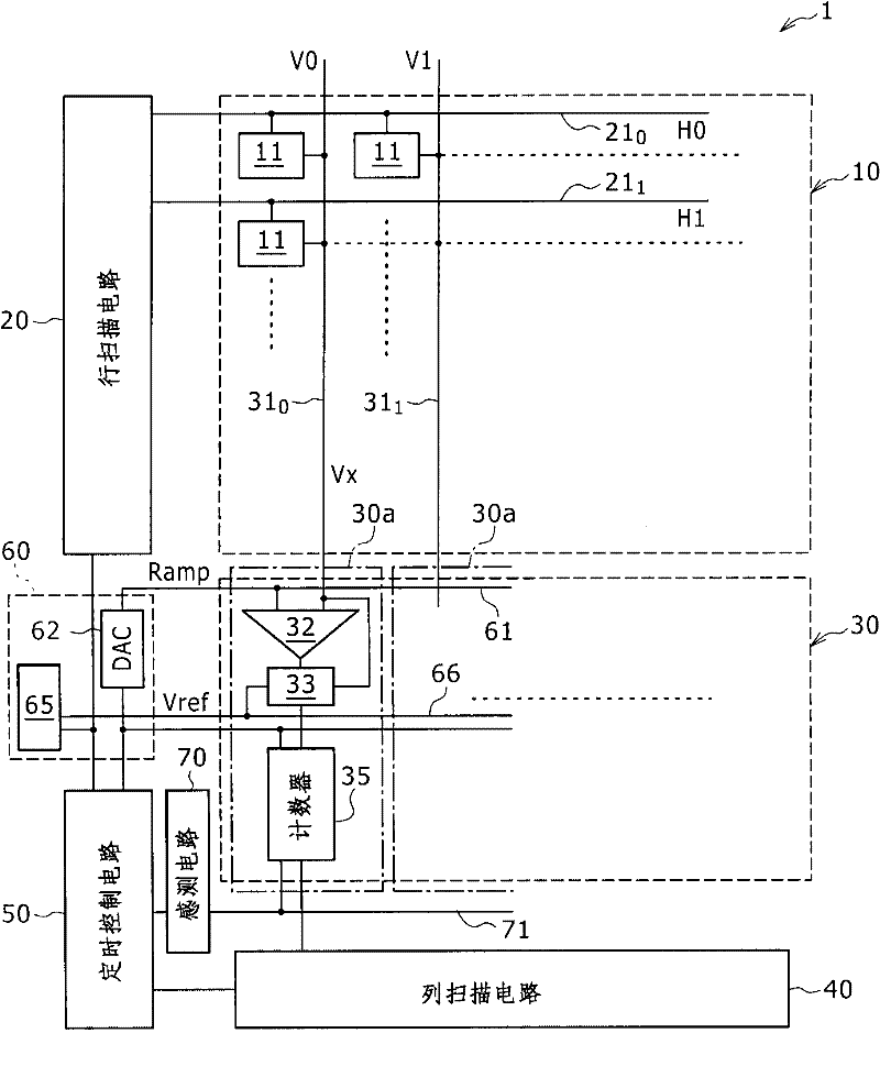
[0043] Hereinafter, embodiments for carrying out the present invention will be described with reference to the drawings. figure 1 is a block diagram of a column ADC type CMOS image sensor including a column-parallel analog / digital conversion section, illustrating an example of a solid-state imaging device according to the present invention. First, refer to figure 1 The overall configuration of the solid-state imaging device 1 will be described.

[0044] 1. Overall configuration of the solid-state imaging device

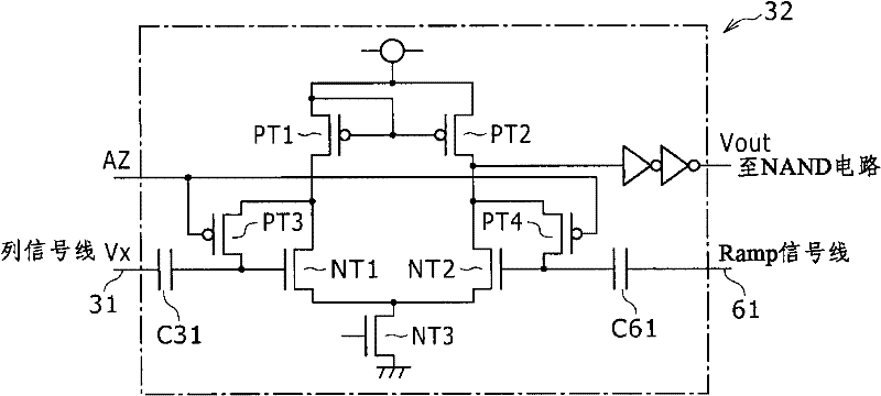
[0045] The solid-state imaging device 1 includes a pixel array 10 , a row scanning circuit 20 , a conversion unit group 30 , a column scanning circuit 40 , a timing control circuit 50 , a reference signal generating circuit 60 , a sensing circuit 70 and the like.

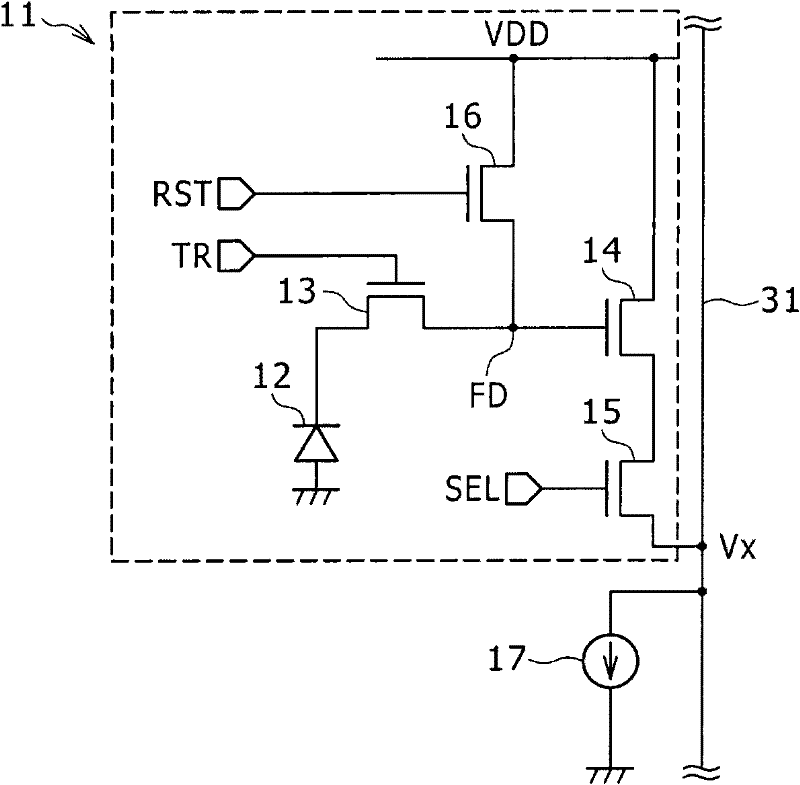
[0046] The pixel array 10 is constituted by arranging a plurality of pixels 11 along a plurality of rows H and columns V in a matrix, and forming a two-dimensional planar imaging section composed of a l...


PUM


Abstract

The present invention provides a solid-state imaging device including: a comparison section that compares a pixel signal from a pixel with a ramp signal and outputs a comparison signal; a measurement section that starts counting in synchronization with the ramp signal, and is supplied to Counting is continued until the signal of the measuring section is reversed to measure the comparison time; the comparator output control section, which is located between the output of the comparing section and the input of the measuring section, if when counting is started, the pixel signal value exceeds The predetermined value determined by the phenomenon, then when the comparison signal is supplied to the measurement part to invert the comparison signal, the comparator output control part stops counting, however, if the pixel signal value does not exceed the predetermined value, it will The non-inverted signal is supplied to the measurement part to continue counting during the measurement period. This solid-state imaging device can correct the blackening phenomenon with a small-scale circuit configuration.

Description

[0001] Cross References to Related Applications [0002] This application contains subject matter related to and claims priority from Japanese Patent Application JP2010-143459 filed in the Japan Patent Office on Jun. 24, 2010, the entire content of which is hereby incorporated by reference. technical field [0003] The present invention relates to a solid-state imaging device. Background technique [0004] As solid-state imaging devices, CCD (Charge Coupled Device) image sensors and CMOS (Complementary Metal Oxide Semiconductor) image sensors are known to the public. The solid-state imaging devices described above are widely used as imaging devices for digital video cameras, digital still cameras, and cellular phones. In recent years, efforts have been made to develop CMOS image sensors whose power consumption is lower than that of CCD image sensors. [0005] As the CMOS image sensor, an image sensor called a column-parallel AD conversion type or a column ADC (Analog-Digit...

Claims


Application Information

Patent Timeline
Patent Type & Authority Applications(China)
IPC IPC(8): H04N5/374H04N5/3745H04N5/378H04N5/359
CPCH04N5/3745H04N5/378H04N5/3598H04N25/627H04N25/77H04N25/75
Inventor 栗原纯一境直史
Owner SONY CORP
Why Eureka
Try Eureka