Magnetron and thin film deposition treatment equipment applying same

A magnetron and magnet technology, applied in the field of microelectronics, can solve problems such as poor uniformity, hindering the continuous filling of pores, and difficulty in controlling the operation accuracy, so as to ensure uniformity and symmetry, improve uniformity and symmetry, and ensure The effect of scan accuracy

Active Publication Date: 2012-01-11
BEIJING NAURA MICROELECTRONICS EQUIP CO LTD
View PDF4 Cites 1 Cited by
  • Summary
  • Abstract
  • Description
  • Claims
  • Application Information

AI Technical Summary

Problems solved by technology

However, traditional sputtering technology cannot control the deposition direction of sputtered particles, so it cannot successfully fill via holes and narrow trenches with large depth / width ratios
like figure 1 As shown, when the traditional sputtering process is used for pore filling, it is easy to have such a problem: that is, when the filling at the bottom corner of the pore has not been completed, a large amount of filler (called top in the industry) has accumulated at the top corner of the pore. suspension phenomenon) to completely close the pores, thus hindering the continuous filling of the pores
However, after the operation speed of the magnet group is greatly increased, it is difficult to control its operation accuracy. If the operation accuracy of the magnet group cannot be guaranteed, it will not be possible to obtain a uniform magnetic field distribution on the target surface, which will affect the overall metal ionization of the target. Uniformity of
However, if the operating speed of the magnet group is not increased, the scanning period of the magnet group will inevitably be extended, which may lead to a situation where the process duration is shorter than the scanning period of the magnet group, that is, the magnet group only scans part of the target area at the end of the process , the metal ionization rate of the scanned target area is significantly higher than that of the unscanned target area, correspondingly, the pore filling of the scanned target area corresponding to the substrate area The uniformity will also be better, but the uniformity of pore filling in the substrate area corresponding to the unscanned target area is relatively poor; it will seriously affect the overall pore filling quality of the substrate
Therefore, the magnetron with the above-mentioned structure will not be able to meet the sputtering process requirements for large-size substrates, especially substrates with a size of 450mm and above.

Method used


Image

  • Magnetron and thin film deposition treatment equipment applying same
  • Magnetron and thin film deposition treatment equipment applying same
  • Magnetron and thin film deposition treatment equipment applying same

Examples


Embodiment Construction

[0038] In order to enable those skilled in the art to better understand the technical solution of the present invention, the magnetron provided by the present invention and the thin film deposition processing equipment using the magnetron will be described in detail below with reference to the accompanying drawings.

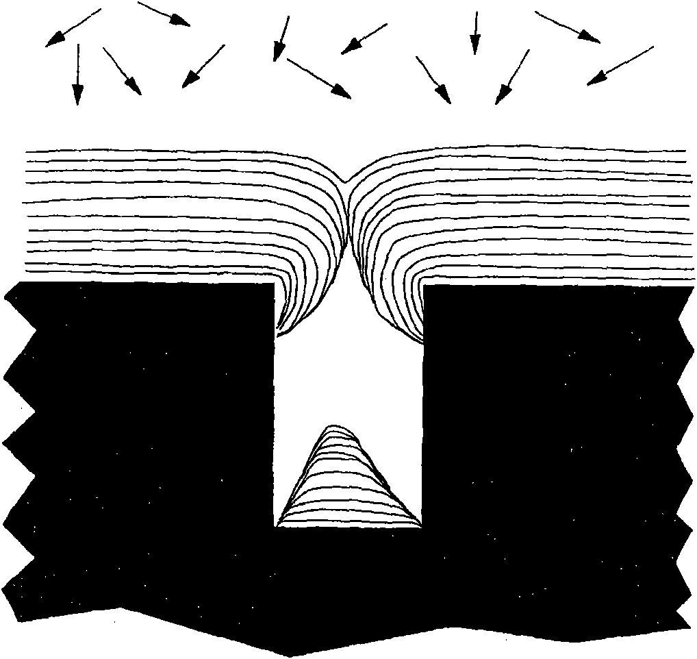
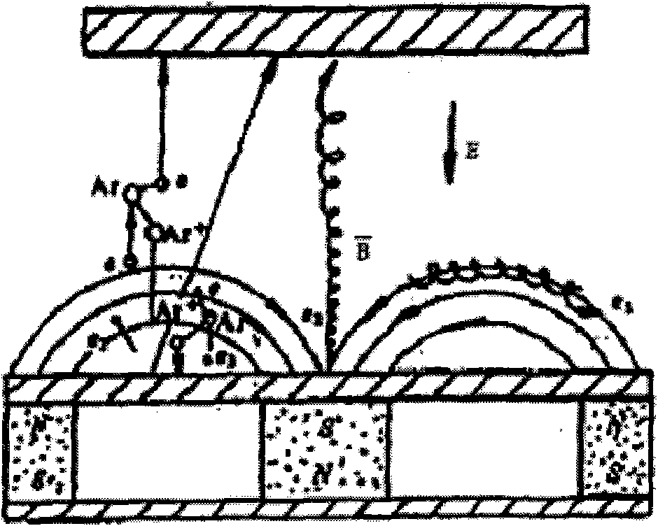
[0039] The magnetron provided by the present invention is used to form a uniformly distributed magnetic field on the surface of a target in a plasma sputtering process, thereby increasing the ionization rate of metal atoms. The magnetron includes: a central magnetron subregion, which has a central magnet group corresponding to the magnetic field applied to the central region of the target; an edge magnetron subregion, which is arranged around the central magnetron subregion, and has a magnetic field corresponding to the target edge region. The edge magnet group of magnetic field; Drive mechanism, it comprises the center drive mechanism that is connected with cente...


PUM


Abstract

The invention provides a magnetron, which comprises a center magnetic control partition, an edge magnetic control partition and a driving mechanism, wherein the driving mechanism can synchronously or independently drive magnetic body groups in the center magnetic control partition and the edge magnetic control partition and make the magnetic body groups run in the own magnetic control partition according to predetermined tracks. The magnetron can effectively increase the metal atom ionization rate of the whole target region, particularly an edge region, so as to improve the hole filling uniformity of the edge region of a substrate. Furthermore, the invention also provides thin film deposition treatment equipment applying the magnetron.

Description

technical field [0001] The invention relates to the technical field of microelectronics, in particular to a magnetron and thin film deposition processing equipment using the magnetron. Background technique [0002] In modern industry, the level of microelectronics processing technology has made unprecedented achievements. An integrated circuit is a typical microelectronic product. It processes microstructures such as pores and trenches of various shapes on a silicon wafer, and then forms tiny transistors by filling the pores and trenches with different materials. Microelectronic components, and connect each microelectronic component according to different electrical characteristics through the metal interconnection layer, and finally form a large-scale integrated circuit. Among them, the production process of metal interconnection layers such as copper and aluminum involved in the production process of integrated circuits needs to be realized by sputtering technology. [0...

Claims


Application Information

Patent Timeline
Patent Type & Authority Applications(China)
IPC IPC(8): H01J25/50H01J37/34
Inventor 杨柏
Owner BEIJING NAURA MICROELECTRONICS EQUIP CO LTD
Why Eureka
Try Eureka