P-i-n type InGaN solar cell possessing superlattice structure

A p-i-n, solar cell technology, applied in circuits, photovoltaic power generation, electrical components, etc., can solve the problem that the conversion efficiency cannot be significantly improved.

Inactive Publication Date: 2012-01-11
XIDIAN UNIV
View PDF1 Cites 22 Cited by
  • Summary
  • Abstract
  • Description
  • Claims
  • Application Information

AI Technical Summary

Problems solved by technology

However, since none of them can meet the requirements of simultaneous increase of open circuit

Method used


Image

  • P-i-n type InGaN solar cell possessing superlattice structure
  • P-i-n type InGaN solar cell possessing superlattice structure
  • P-i-n type InGaN solar cell possessing superlattice structure

Examples


Embodiment 1

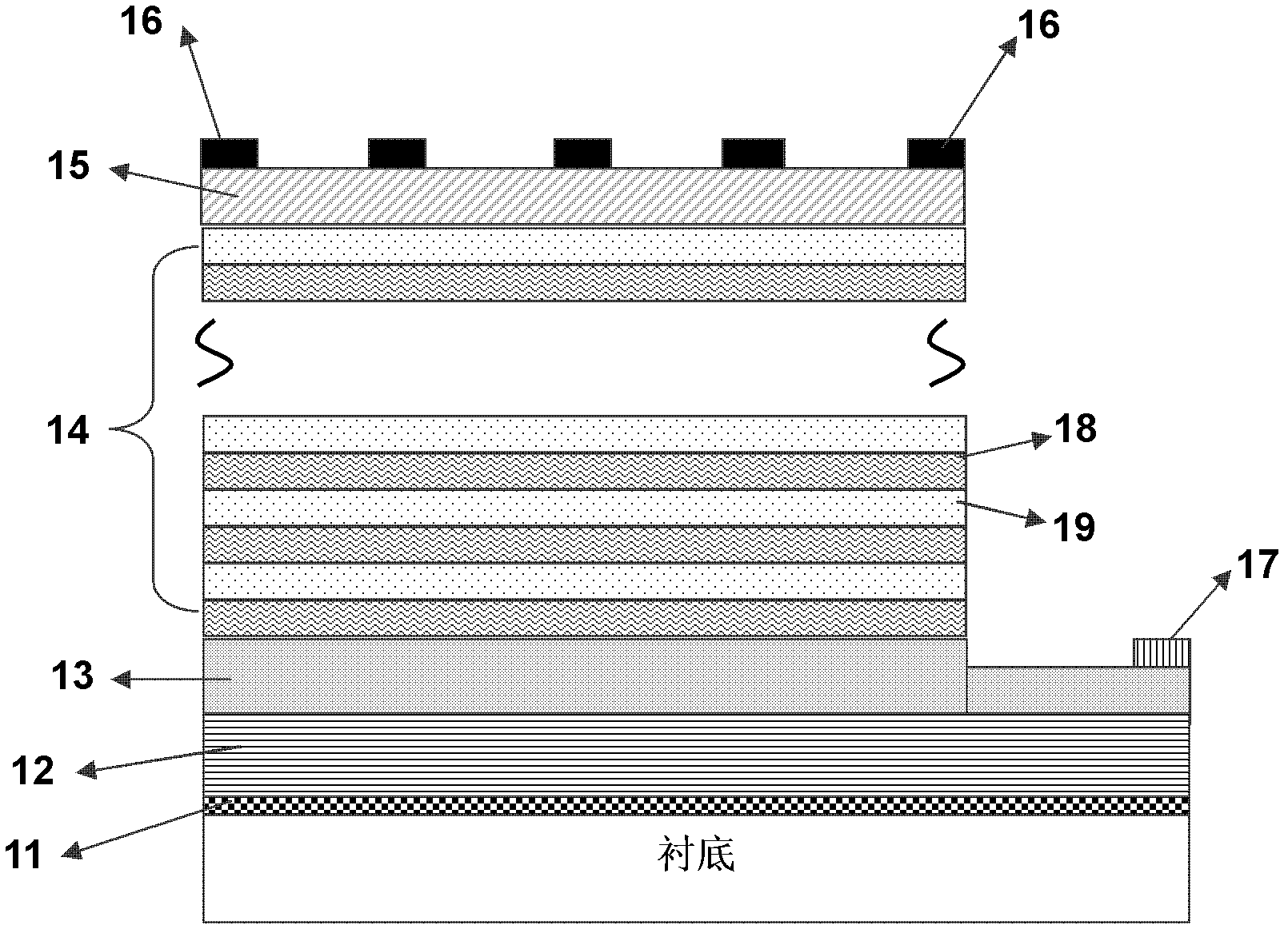
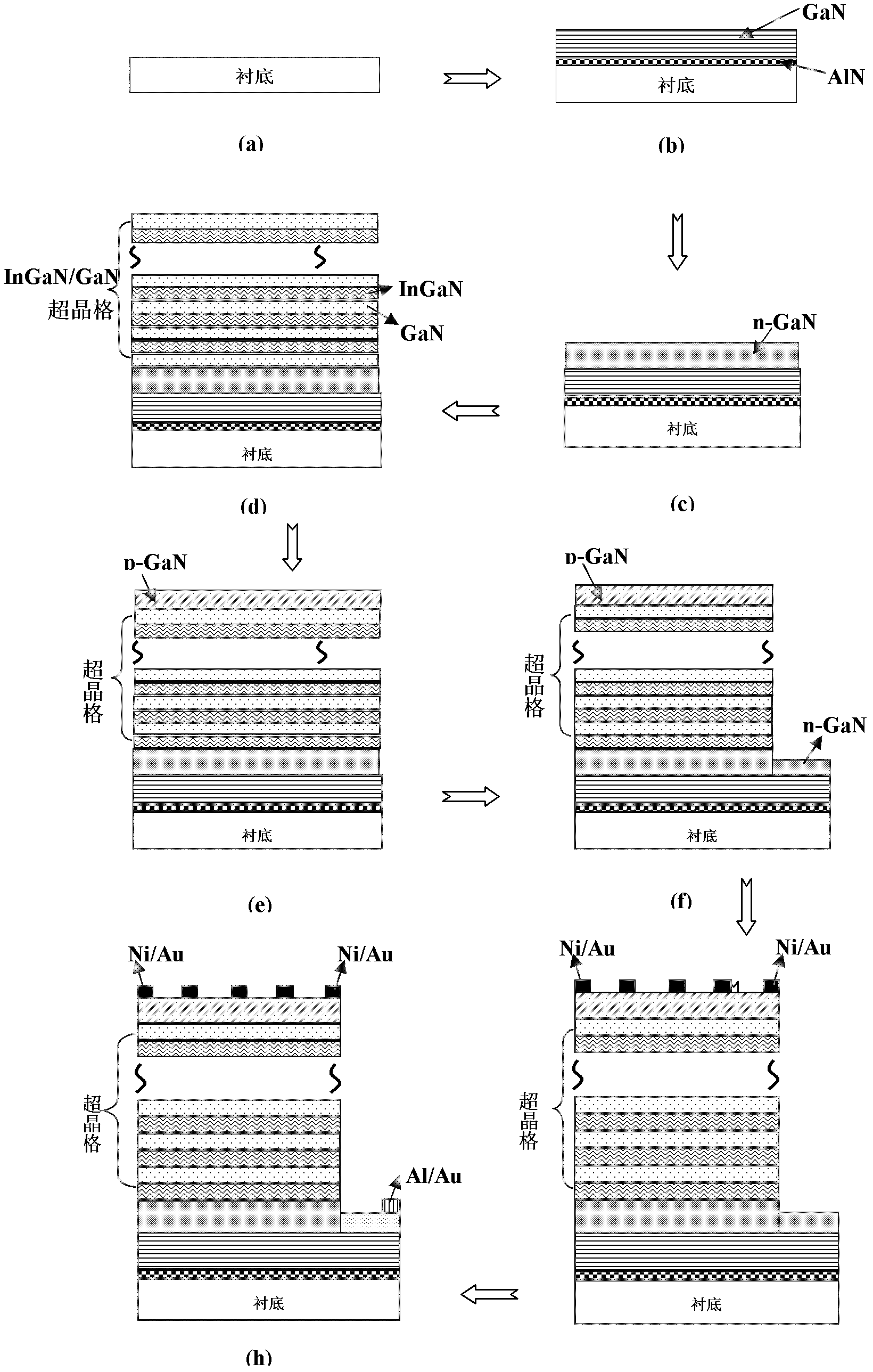
[0035] The p-i-n type InGaN solar cell containing the superlattice structure of the present invention comprises: sapphire substrate, AlN nucleation layer 11, GaN buffer layer 12, n-GaN layer 13, InGaN / GaN superlattice 14 and p-GaN layer 15 . Among them, the AlN nucleation layer 11 is grown at high temperature; the GaN buffer layer 12 is an unintentionally doped layer; the thickness of the n-GaN13 layer is 50nm, and the electron concentration is 1×10 18 / cm 3 ; The InGaN / GaN superlattice 14 has 8 periods, each period is composed of a well layer InGaN18 with a thickness of 8nm and a barrier layer GaN19 with a thickness of 3nm, both InGaN and GaN are intrinsic thin films, and the carrier concentration is 1× 10 16 / cm 3 , the In composition in the well layer InGaN is 15%; the thickness of the p-GaN layer 15 is 50nm, and the hole concentration is 1×10 17 / cm 3 . Grid Ni / Au ohmic electrodes 16 are distributed on the surface of p-GaN layer 15 , each electrode has a width of 1 μ...

Embodiment 2

[0037] The p-i-n type InGaN solar cell containing the superlattice structure of the present invention comprises, from bottom to top, a silicon substrate, an AlN nucleation layer 11, a GaN buffer layer 12, an n-GaN layer 13, an InGaN / GaN superlattice 14 and p-GaN layer 15 . Among them, the AlN nucleation layer 11 is grown at high temperature; the GaN buffer layer 12 is an unintentionally doped layer; the thickness of the n-GaN13 layer is 50nm, and the electron concentration is 1×10 18 / cm 3 ; The InGaN / GaN superlattice 14 has 14 periods, each period is composed of a well layer InGaN18 with a thickness of 14nm and a barrier layer GaN19 with a thickness of 5nm, both InGaN and GaN are intrinsic thin films, and the carrier concentration is 6× 10 16 / cm 3, the In composition in the well layer InGaN is 40%; the thickness of the p-GaN layer 15 is 50nm, and the hole concentration is 1×10 17 / cm 3 . The surface of the p-GaN layer 15 is distributed with grid-shaped ITO electrodes 1...

Embodiment 3

[0039] The p-i-n type InGaN solar cell containing the superlattice structure of the present invention comprises: sapphire substrate, AlN nucleation layer 11, GaN buffer layer 12, n-GaN layer 13, InGaN / GaN superlattice 14 and p-GaN layer 15 . Among them, the AlN nucleation layer 11 is grown at high temperature; the GaN buffer layer 12 is an unintentionally doped layer; the thickness of the n-GaN13 layer is 50nm, and the electron concentration is 1×10 18 / cm 3 ; The InGaN / GaN superlattice 14 has 14 periods, each period is composed of a well layer InGaN18 with a thickness of 16nm and a barrier layer GaN19 with a thickness of 8nm, both InGaN and GaN are intrinsic thin films, and the carrier concentration is 2× 10 17 / cm 3 , the In composition in the well layer InGaN is 90%; the thickness of the p-GaN layer 15 is 50nm, and the hole concentration is 1×10 17 / cm 3 . Grid Ni / Au ohmic electrodes 16 are distributed on the surface of p-GaN layer 15 , each electrode has a width of 2...


PUM

PropertyMeasurementUnit
Thicknessaaaaaaaaaa
Thicknessaaaaaaaaaa
Thicknessaaaaaaaaaa

Abstract

The invention discloses a p-i-n type InGaN solar cell possessing a superlattice structure. The current p-i-n type InGaN solar cell possesses a problem of low conversion efficiency. The p-i-n type InGaN solar cell provided in the invention can solve the above problem. The solar cell comprises, from bottom to top: a substrate; an AlN nucleating layer (11), which is growth at a high temperature; an unintended doped GaN buffer layer (12); an n-GaN layer (13) possessing a thickness of 50-100nm and an electron concentration of 1x10¹⁸-6x10¹⁹/cm<3>; a InGaN/GaN superlattice structure (14) possessing a period of 8-30; a p-GaN layer (15) possessing the thickness of 50-100nm and a hole concentration of 1x10¹⁷-6x10¹⁸/ cm<3>. The thickness of a trap layer InGaN (18) of the InGaN/GaN superlattice is 8-16nm. In ingredients are 15%-90%. The thickness of a barrier layer GaN (19) is 3-8nm. The concentration of carriers is 1x10¹⁶-2x10¹⁷/ cm<3>. Grid-shaped Ni/Au ohmic electrodes (16) are distributed on the surface of a P-GaN layer (15). An Al/Au ohmic electrode (17) is led out from a right side of the surface of the n-GaN layer (13). By using the solar cell of the invention, a short circuit current of the cell can be raised. The solar cell possesses high conversion efficiency and can be used for solar photovoltaic power generation.

Description

technical field [0001] The invention belongs to the field of semiconductor photovoltaic devices, and relates to a p-i-n type InGaN solar cell containing a superlattice structure, which can be used for solar photovoltaic power generation and development and utilization of new energy. Background technique [0002] With the global energy crisis and the deterioration of ecological environment problems, solar energy, as an "inexhaustible and inexhaustible" clean energy, has attracted more and more attention. As early as 1954, Bell Laboratories in the United States first successfully developed the first practical crystalline silicon pn junction solar cell, and soon applied it to space technology. In 1973, the oil crisis broke out. Since then, people have generally paid more and more attention to solar cells. Some developed countries have formulated a series of preferential policies to encourage photovoltaic power generation, and implemented huge photovoltaic engineering plans, cr...

Claims


Application Information

Patent Timeline
IPC IPC(8): H01L31/0352H01L31/075H01L31/18
CPCY02E10/50Y02E10/548Y02P70/50
Inventor 郝跃毕臻周小伟张进成王冲马晓华
Owner XIDIAN UNIV
Why Eureka
Try Eureka