FPGA (Field Programmable Gate Array)-based single event effect test system for NAND FLASH device

A technology for testing systems and devices under test, applied in the direction of instruments, static memory, etc., can solve problems such as complex and inability to achieve testing, and achieve the effect of improving accuracy

Active Publication Date: 2012-01-25
NO 510 INST THE FIFTH RES INST OFCHINA AEROSPAE SCI & TECH
View PDF3 Cites 38 Cited by
  • Summary
  • Abstract
  • Description
  • Claims
  • Application Information

AI Technical Summary

Problems solved by technology

Since the structure of NAND Flash devices above 1G is different from other static memory structure...

Method used


Image

  • FPGA (Field Programmable Gate Array)-based single event effect test system for NAND FLASH device
  • FPGA (Field Programmable Gate Array)-based single event effect test system for NAND FLASH device

Examples


Embodiment

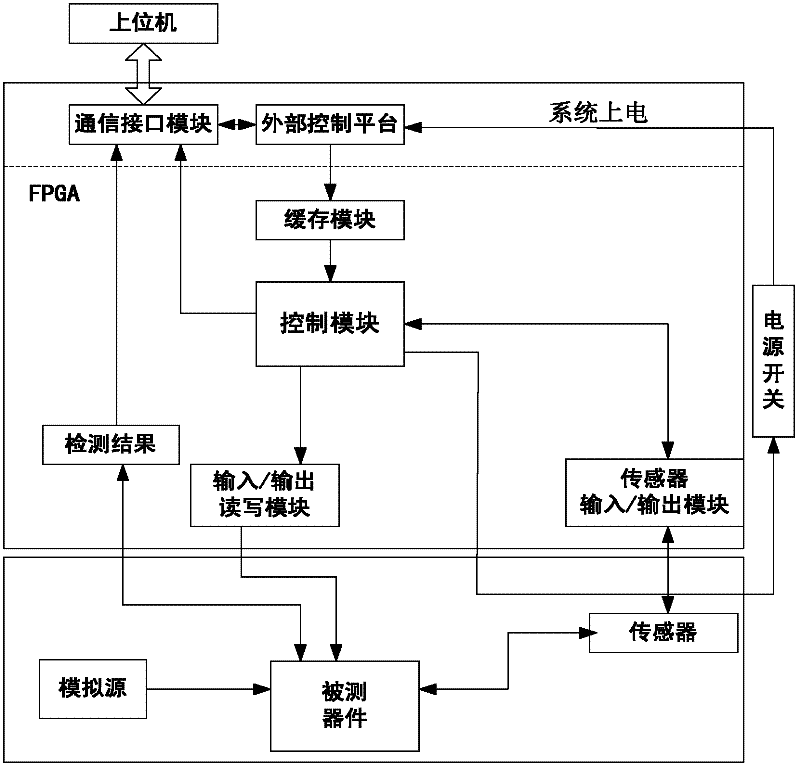
[0049] A kind of NAND FLASH device single event effect test system based on FPGA of the present invention, described system comprises communication interface module, peripheral control platform, host computer, device under test, simulation source, power switch and FPGA, wherein FPGA comprises cache module, Control module, input / output read-write module, sensor input / output module, detection result module;

[0050] The peripheral control platform is connected with the buffer module, the communication interface module and the power switch, the buffer module is connected with the control module, the control module is connected with the input / output read-write module, the power switch, the communication interface module and the sensor input / output module, and the sensor input / output The output module is connected to the sensor, and the device under test is connected to the analog source, sensor, input / output read-write module and the test result module at the same time. The test resu...


PUM


Abstract

The invention discloses an FPGA (Field Programmable Gate Array)-based single event effect test system for a NAND FLASH device and belongs to the technical field of space radiation effect and reinforcement technology. The system comprises a communication interface module, a peripheral control platform, an upper computer, a tested device, an analog source, a power switch and an FPGA, wherein the FPGA comprises a cache module, a control module, an input/ output reading and writing module, a sensor input/ output module and a detection result module. The system can be used for testing the single event effect of a large-capacity NAND FLASH device to obtain single event effect characteristic parameters, and further the anti-single event effect capability of the tested device can be estimated through the analysis on the obtained parameters.

Description

technical field [0001] The invention relates to an FPGA-based NAND FLASH device single event effect test system, belonging to the field of space radiation effect and reinforcement technology. Background technique [0002] Because NAND Flash memory has the advantages of low power consumption, good chip pin compatibility, no loss of data after power failure, and no need to re-refresh data in a short period of time, etc., it has been used in space in recent years. However, charged particles in the space radiation environment can easily induce single event effects in NAND Flash devices, which will have a certain impact on the on-orbit performance of satellite payloads. At the same time, with the requirements of long life and high reliability of satellites, the evaluation of ground single event effect test of devices is particularly important. Since the structure of NAND Flash devices above 1G is different from other static memory structures in the past and is more complicated, ...

Claims


Application Information

Patent Timeline
IPC IPC(8): G11C29/56
Inventor 薛玉雄安恒杨生胜王德坤曹洲把得东石红汤道坦李存惠
Owner NO 510 INST THE FIFTH RES INST OFCHINA AEROSPAE SCI & TECH
Why Eureka
Try Eureka