QFN (quad flat non-lead) package with multiple circles of pins and manufacturing method thereof

A leadless packaging, flat four-sided technology, applied in semiconductor/solid-state device manufacturing, electrical components, electrical solid-state devices, etc., can solve the problems of lead frame and plastic packaging material falling off, unable to meet high density, shortened cutting blade life, etc. Achieve the effect of improving bonding quality and surface mount quality, preventing metal burrs, and improving cutting efficiency

Inactive Publication Date: 2012-02-01
BEIJING UNIV OF TECH
View PDF8 Cites 18 Cited by
  • Summary
  • Abstract
  • Description
  • Claims
  • Application Information

AI Technical Summary

Benefits of technology

This patented technology allows for better placement of metallic leads within an electronic device's housing by creating step structures that increase their contact areas between them and other components such as conductors. These steps help keep water out without getting trapped under certain parts like solder joints. Additionally, this design prevents damage caused by external factors (such as impact) while also allowing for efficient use of space due to its small size. Overall, these technical improvements make it easier and more reliable to manufacturers produce high-quality electronics devices at competitive prices over conventional methods.

Problems solved by technology

This patented technical problem addressed in this patents relates to improving the quality, functionality, durability, flexibility, weight reduction, thinning, space utilizing capacity, production speed, and costs associated with semiconductor devices like integrated circuits (Integrated Circuit). Current methods involve attaching lead frames onto printed circuit boards (PCB), making them thinner than usual ones without any extra parts attached thereto, reducing their overall thicknesses, increasing cool resistance, lower resistances, enhancing signal transmission capabilities, protecting against damage caused by external factors like humid environments, allowing better temperature management, minimizing interference signals, maintaining long lifetimes, and ensures reliable operation over longer periods of time.

Method used


Image

  • QFN (quad flat non-lead) package with multiple circles of pins and manufacturing method thereof
  • QFN (quad flat non-lead) package with multiple circles of pins and manufacturing method thereof
  • QFN (quad flat non-lead) package with multiple circles of pins and manufacturing method thereof

Examples


Embodiment Construction

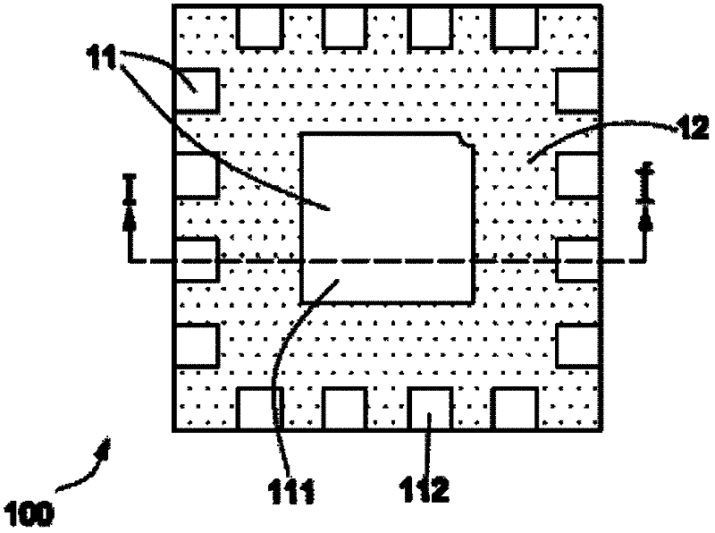
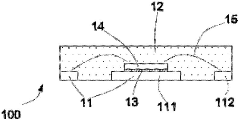
[0058] The present invention is described in detail below in conjunction with accompanying drawing:

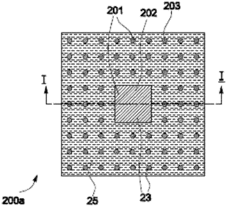
[0059] Figure 2A A schematic diagram of the rear side of a QFN package structure in which the cross-section of the pins is circular and the pins on each side of the chip carrier are arranged in parallel according to the embodiment of the present invention. Figure 2B A schematic diagram of the back side of a QFN package structure in which the cross-section of the pins is rectangular and the pins on each side of the chip carrier are arranged in parallel according to the embodiment of the present invention.

[0060] Refer to the above Figure 2A -B It can be seen that, in this embodiment, the lead frame 201 of the multi-turn pin arrangement QFN package structure 200a and 200b includes a chip carrier 202 and pins 203 arranged in multi-turn around the chip carrier 202, and the chip carrier 202 is each The side pins 203 are arranged in parallel, the metal material layer 23 is ar...


PUM


Abstract

The invention discloses a QFN (quad flat non-lead) package with multiple circles of pins and a manufacturing method thereof. The package comprises a lead frame, metal material layers, an IC (integrated circuit) chip, an insulated filling material, an adhesive material, metal conductors and a plastic package material, wherein the lead frame comprises a chip carrier and multiple pins which are arranged around the chip carrier for multiple circles; the metal material layers are arranged on the upper surface and lower surface of the lead frame; the IC chip is arranged on the metal material layer on the upper surface of the lead frame; the insulated filling material is arranged below a stepped structure of the lead frame; the adhesive material is arranged between the IC chip and the metal material layer on the upper surface of the lead frame; the IC chip is respectively connected with inner pins of the multiple circles of pins and the upper surface of the chip carrier by the metal conductors; and the plastic package material coats and seals the IC chip, the adhesive material, the metal conductors, parts of regions of the lead frame and parts of metal material layer. According to the invention, the bottleneck of the low I/O (input/output) quantity can be broken through, and the sealing reliability is improved.

Description


Claims


Application Information

Patent Timeline
Owner BEIJING UNIV OF TECH
Why Eureka
Try Eureka