Nanoimprint lithography machine for whole wafer

A technology of nanoimprinting and lithography machine, applied in the direction of optomechanical equipment, microlithography exposure equipment, optics, etc., can solve problems such as no one is ideal, substrate breakage, etc., and achieve easy complete contact and high productivity , Eliminate the effect of "bubble" defect

Active Publication Date: 2013-04-10
QINGDAO TECHNOLOGICAL UNIVERSITY
View PDF1 Cites 0 Cited by
  • Summary
  • Abstract
  • Description
  • Claims
  • Application Information

AI Technical Summary

Problems solved by technology

However, epitaxial growth will lead to more obvious bending of large-scale substrates. In the subsequent lithography process, forced use of vacuum adsorption and other methods to compensate for this bending in exchange for high resolution in lithography may cause substrate breakage.
Therefore, the development of full-chip nanotechnology and equipment for large-size wafers faces many technical difficulties, and there is no ideal solution at present.

Method used


Image

  • Nanoimprint lithography machine for whole wafer
  • Nanoimprint lithography machine for whole wafer
  • Nanoimprint lithography machine for whole wafer

Examples


Embodiment 1

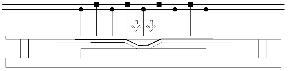
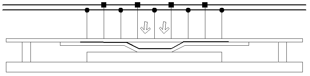
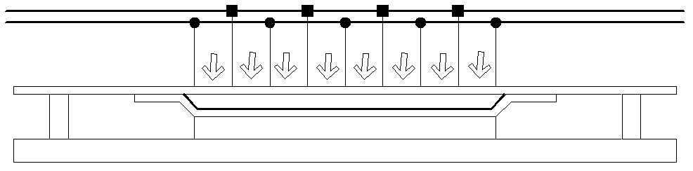
[0058] A full wafer nanoimprint lithography machine, such as figure 2 As shown, it includes: an imprint head 1, an exposure system 2, a template 3, a film holder 4, a demoulding nozzle 5, a frame 6, a marble base 7, a vacuum pipeline 8 and a pressure pipeline 9, wherein the template 3 is fixed on the bottom surface 10104 of the template workbench on the imprint head 1, the film carrier 4 is placed vertically directly below the template 3, and is fixed on the marble base 7, and a demoulding nozzle 5 is arranged around the film carrier; the exposure system 2 The ultraviolet light source is placed in the exposure working room 102 of the imprint head 1, and is located directly above the transparent template workbench 101; B101012, the air inlet C101013 are connected; the vacuum pipeline 8 is connected with the vacuum suction cup 403 on the wafer table 4 and the control valve air inlet II 40402 of the fixed base 401, and the control valve air inlet I 40401; the embossing head 1 is...

Embodiment 2

[0072] Figure 12It is a schematic diagram of the three-dimensional structure of the whole wafer nanoimprint lithography machine in Embodiment 2 of the present invention. The main difference between Embodiment 2 and Embodiment 1 lies in the difference in the mechanism form of the imprint head 1 and the frame 6 .

[0073] Figure 13 It is a schematic diagram of the three-dimensional structure of the double guide rail linear guide of the first scheme of the embodiment 2 of the present invention. It includes a template workbench 101, an exposure studio 102, a flange 103, a ball screw 104, a coupling 105, a servo Motor 106, support adjustment block 109, slide block 1011, small bracket 1012, connector 1013 and guide rail 1014, wherein, exposure studio 102 is connected with template workbench 101 by screws, template workbench 101 is provided with horizontal pipeline 10103 and Vertical pipeline 10102 realizes the uniform distribution of compressed air and vacuum gas on the template ...


PUM

PropertyMeasurementUnit
thicknessaaaaaaaaaa
thicknessaaaaaaaaaa

Abstract

The invention discloses a nanoimprint lithography machine for a whole wafer. The nanoimprint lithography machine comprises a lithography head, an exposure system, a mold plate, a wafer bearing platform, demolding nozzles, a rack, a marble base, a vacuum pipeline and a pressure pipeline, wherein the mold plate is fixed on the lithography head, the wafer bearing platform is arranged below the mold plate exactly and fixed on the marble base, the demolding nozzles are arranged around the wafer bearing platform, an ultraviolet light source of the exposure system is arranged in the lithography head, the vacuum pipeline and the pressure pipeline are both connected with the lithography head, and the vacuum pipeline is also connected with the wafer bearing platform. The invention also provides a method for carrying out nanoimprint lithography on the whole wafer by using the nanoimprint lithography machine. The nanoimprint lithography machine for the whole wafer has the advantages of simple structure, wide adaptability, convenience in operation, low manufacturing cost, high reliability and the like, can be applied to LED (light emitting diode) patterning and the manufacture of microlenses and microfluid devices, especially suitable for the low-cost and large-scale manufacture of a photonic crystal LED.

Description

technical field [0001] The invention relates to a nano-imprint photolithography machine, in particular to a single-step whole wafer nano-imprint photolithography machine, which belongs to the technical field of micro-nano manufacturing and photolithography. Background technique [0002] Nanoimprint lithography (Nanoimprint Lithography, NIL) is a new micro-nano patterning method, which is a technology that uses a mold to realize its patterning through the force deformation of the resist. Compared with other micro-nano manufacturing methods, NIL has the characteristics of high resolution, ultra-low cost (NIL at the same production level assessed by international authoritative organizations is at least an order of magnitude lower than traditional optical projection lithography) and high productivity, especially in large-area micro-nano It has outstanding advantages in the manufacture of nanostructures and complex three-dimensional micro-nanostructures. With the wide applicatio...

Claims


Application Information

Patent Timeline
Patent Type & Authority Patents(China)
IPC IPC(8): G03F7/00G03F7/20
Inventor 兰红波丁玉成
Owner QINGDAO TECHNOLOGICAL UNIVERSITY
Why Eureka
Try Eureka