Three-dimensional multivalue nonvolatile memory structure

A non-volatile, memory technology, used in semiconductor devices, electric solid state devices, semiconductor/solid state device manufacturing, etc., to achieve the effect of being conducive to wide application, improving storage density, and optimizing programming

Inactive Publication Date: 2012-02-08
INST OF MICROELECTRONICS CHINESE ACAD OF SCI
View PDF2 Cites 4 Cited by
  • Summary
  • Abstract
  • Description
  • Claims
  • Application Information

AI Technical Summary

Problems solved by technology

The storage density of the storage arrays described in the above patents has room for further improvement

Method used


Image

  • Three-dimensional multivalue nonvolatile memory structure
  • Three-dimensional multivalue nonvolatile memory structure
  • Three-dimensional multivalue nonvolatile memory structure

Examples


Embodiment Construction

[0030] In order to make the object, technical solution and advantages of the present invention clearer, the present invention will be described in further detail below in conjunction with specific embodiments and with reference to the accompanying drawings.

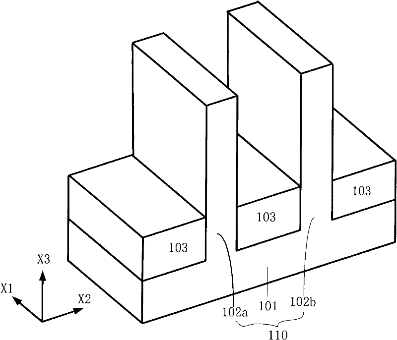
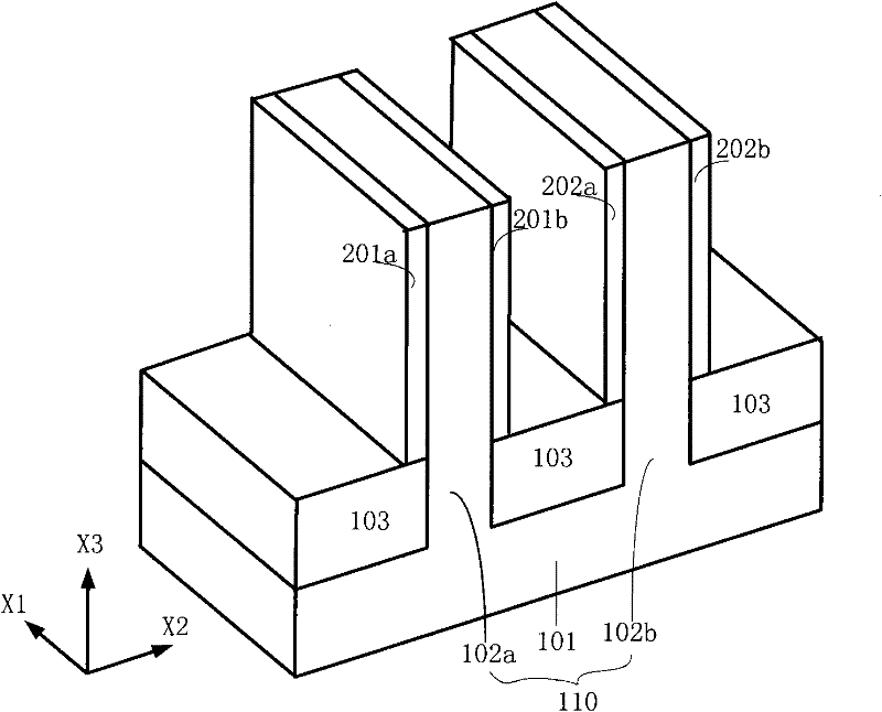
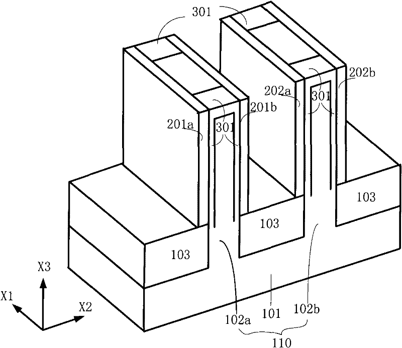
[0031] The three-dimensional multi-value non-volatile memory structure provided by the present invention has a three-dimensional structure based on the characteristics of charge local storage, and each unit has four physical storage points, thereby realizing the characteristics of multi-value storage. Based on the three-dimensional structure of a single device, it can Realize three-dimensional integration of memory arrays, thereby greatly improving storage density. The structure specifically includes: a Fin structure connected to a semiconductor substrate; a tunnel dielectric layer, a charge trapping layer, and a charge blocking layer sequentially formed on the side walls of the Fin structure; periodic source and drain reg...


PUM


Abstract

The invention discloses a three-dimensional multivalue nonvolatile memory structure, which comprises Fin structures, a tunneling dielectric layer, a charge capture layer and a charge barrier layer, and periodic source and drain regions, wherein the Fin structures are connected with a semiconductor substrate; the tunneling dielectric layer, the charge capture layer and the charge barrier layer are formed on the side walls of the Fin structures sequentially; the periodic source and drain regions are formed on the Fin structures; control grid electrodes are exported from a position between adjacent Fin structures; and the grid electrodes in a vertical direction are isolated by the dielectric layer, and sources and drains are exported from the tops of the Fin structures, so three-dimensional integration can be formed. The three-dimensional multivalue nonvolatile memory structure is high in density and easy to integrate and can be implemented by adopting the conventional memory manufacturing process; and popularization and application of the three-dimensional multivalue nonvolatile memory structure is facilitated.

Description

technical field [0001] The invention relates to the technical field of microelectronics manufacturing and memory, in particular to a multi-value non-volatile memory structure with three-dimensional integration characteristics and localized storage charge. Background technique [0002] The current microelectronics products are mainly divided into two categories: logic devices and storage devices, and storage devices are needed in almost all electronic products today, so storage devices occupy a very important position in the field of microelectronics. Storage devices can generally be classified into volatile memories and non-volatile memories. The main feature of non-volatile memory is the ability to retain stored information for a long period of time without power on. It not only has the characteristics of read-only memory (ROM), but also has high access speed, and is easy to erase and rewrite, and consumes less power. With the demand for large-capacity and low-power stora...

Claims


Application Information

Patent Timeline
Patent Type & Authority Applications(China)
IPC IPC(8): H01L27/115H01L21/8247
Inventor 刘明朱晨昕霍宗亮王琴龙世兵
Owner INST OF MICROELECTRONICS CHINESE ACAD OF SCI
Why Eureka
Try Eureka