Manufacturing method based on control over angle of contact hole wall of liquid crystal display device

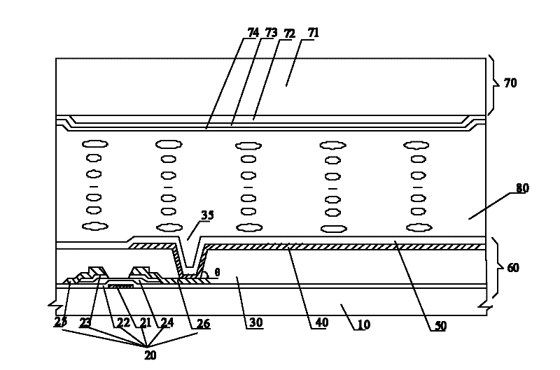
A technology of a liquid crystal display device and a manufacturing method is applied in the field of manufacturing the angle of the wall of the contact hole of the liquid crystal display device, and can solve the problems of inability to accurately control the angle of the contact hole 35, the area is too large, and the aperture ratio is affected.

Inactive Publication Date: 2012-02-29
SHENZHEN CHINA STAR OPTOELECTRONICS TECH CO LTD
View PDF3 Cites 2 Cited by
  • Summary
  • Abstract
  • Description
  • Claims
  • Application Information

AI Technical Summary

Problems solved by technology

[0013] In the above-mentioned manufacturing method, the inclination angle of the hole wall of the contact hole is formed by baking, and the angle of the contact hole 35 cannot be accurately controlled. When the inclination angle of the hole wall of the contact hole 35 is less than 45 degrees, the area of ​​the contact hole 35 will be too large. Reducing the aperture ratio affects the brightness, and when the inclination angle of the wall of the contact hole 35 is greater than 70 degrees, it will cause uneven coating and defects in the next ITO process.

Method used


Image

  • Manufacturing method based on control over angle of contact hole wall of liquid crystal display device
  • Manufacturing method based on control over angle of contact hole wall of liquid crystal display device
  • Manufacturing method based on control over angle of contact hole wall of liquid crystal display device

Examples


Embodiment Construction

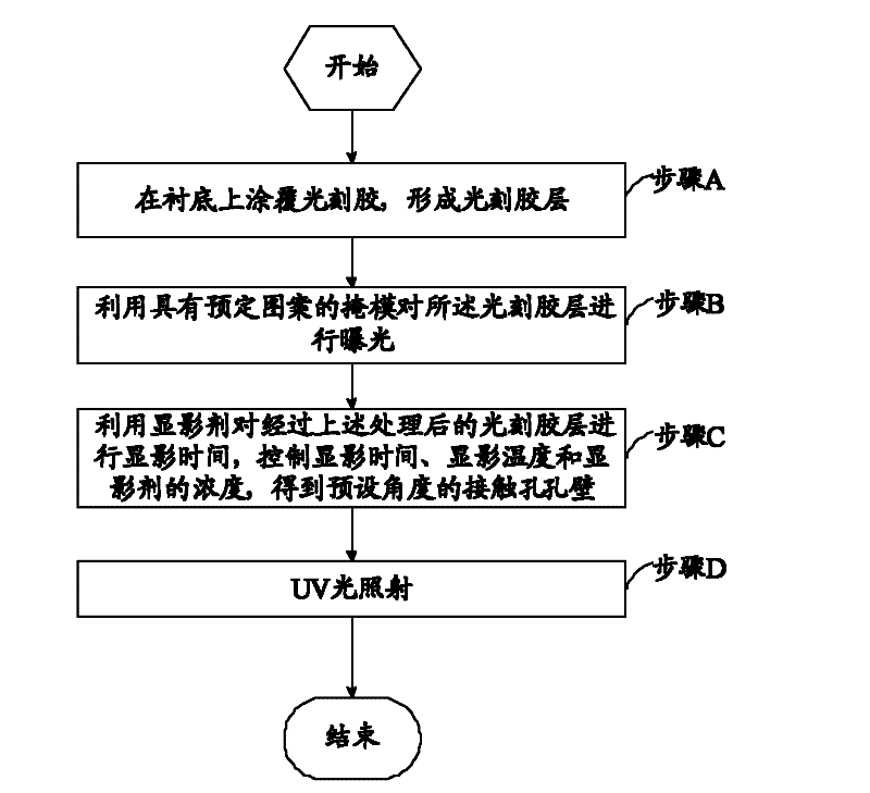
[0037] It should be understood that the specific embodiments described here are only used to explain the present invention, not to limit the present invention.

[0038] As we all know, photoresist is a photosensitive material temporarily coated on the wafer, similar to the photosensitive material of the negative film, and a chemical reaction occurs after being irradiated, thereby transferring the optical pattern on the photomask to the wafer surface. In the process of forming the contact hole pattern, a positive photoresist is generally used due to its high resolution requirements. This type of photoresist is usually a phenolic resin (Novolac) crosslinked by a photosensitive agent. When exposed to light, photons trigger the photosensitive acid generator (PAG) in the photoresist to undergo a photochemical reaction to generate protons H + (photoacid), this proton will react with the photoresist to cause its relationship bond to be broken and decrosslinked, so that the exposed p...


PUM

PropertyMeasurementUnit
thicknessaaaaaaaaaa

Abstract

The invention discloses a manufacturing method based on control over an angle of a contact hole wall of a liquid crystal display device, which comprises the following steps of: (1) coating photoresist to a substrate to form a photoresist layer; (2) exposing the photoresist layer by using a photo-hardening monomer with a preset pattern; and (3) developing the treated photoresist layer by using a developing agent, and controlling developing time, developing temperature and the concentration of the developing agent to obtain a contact hole with preset angle. By using the melting point characteristic of the photoresist material including the photo-hardening monomer, the inclined angle of the contact hole wall is accurately controlled between 45 DEG and 70 DEG.

Description

technical field [0001] The invention relates to the field of liquid crystal display, in particular to a manufacturing method for controlling the wall angle of a contact hole of a liquid crystal display device. Background technique [0002] figure 1 Shown is a sectional view of a prior art liquid crystal panel, referring to figure 1 , the liquid crystal panel includes a TFT substrate 60 , a color filter substrate 70 facing the TFT substrate 60 , and a liquid crystal layer 80 located between the TFT substrate 60 and the color filter substrate 70 . [0003] The TFT substrate 60 includes a first substrate 10 opposite to each other, a TFT 20 formed on the first substrate 10, an organic insulating layer 30 formed on the first substrate 10 with the TFT 20, a pixel electrode 40 formed on the organic insulating layer 30, and The first alignment film 50 is formed on the pixel electrode 40 . [0004] Each TFT 20 includes a gate 21 , a gate insulating layer 22 , an active pattern 23 ...

Claims


Application Information

Patent Timeline
Patent Type & Authority Applications(China)
IPC IPC(8): G02F1/1362H01L21/768G03F7/00
CPCG02F1/136227G03F7/30H01L21/76804
Inventor 吴若杉陈孝贤
Owner SHENZHEN CHINA STAR OPTOELECTRONICS TECH CO LTD
Why Eureka
Try Eureka