Process for making non-void high-reliability convex points in wafer by vacuum brazing

A vacuum and wafer technology, applied in the direction of manufacturing tools, welding equipment, metal processing equipment, etc., can solve the problems that the reliability needs to be further improved

Inactive Publication Date: 2012-03-14
NO 771 INST OF NO 9 RES INST CHINA AEROSPACE SCI & TECH
View PDF5 Cites 11 Cited by
  • Summary
  • Abstract
  • Description
  • Claims
  • Application Information

AI Technical Summary

Problems solved by technology

Regardless of whether heating is performed under a protective atmosphere, it is unavoidable that there will be voids / holes or bubbles in some solder joints after soldering, and the reliability needs to be further improved

Method used


Image

  • Process for making non-void high-reliability convex points in wafer by vacuum brazing
  • Process for making non-void high-reliability convex points in wafer by vacuum brazing
  • Process for making non-void high-reliability convex points in wafer by vacuum brazing

Examples


Embodiment Construction

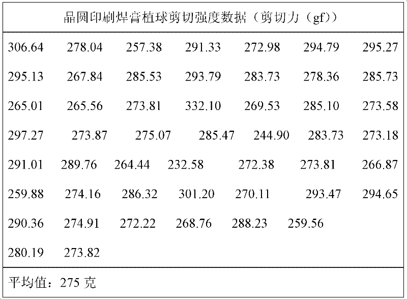
[0010] After cleaning, the assessment measurement is carried out, and the results are as follows:

[0011] A. Shear strength test

[0012] The solder balls on the surface of the chip were subjected to a shear force test, and a total of 50 points were tested. The test values ​​are shown in Table 1.

[0013] Table 1 Shear strength test data table

[0014]

[0015] The shear force value is between 244.90g and 332.10g, with an average value of 275g, which is far greater than the national military standard and meets the use requirements.

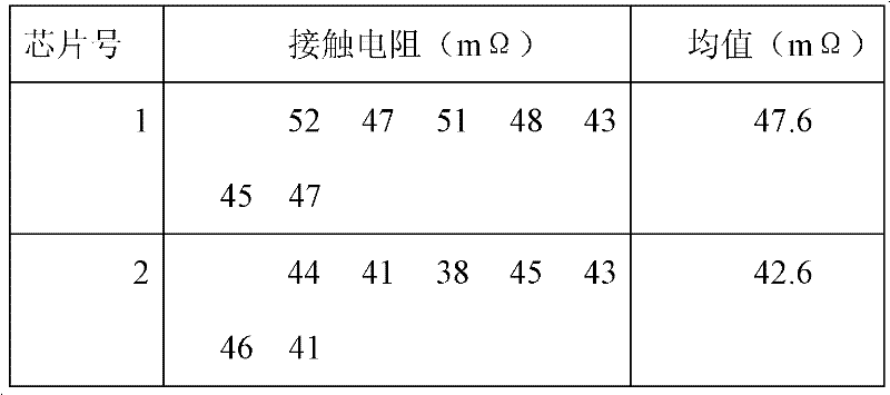
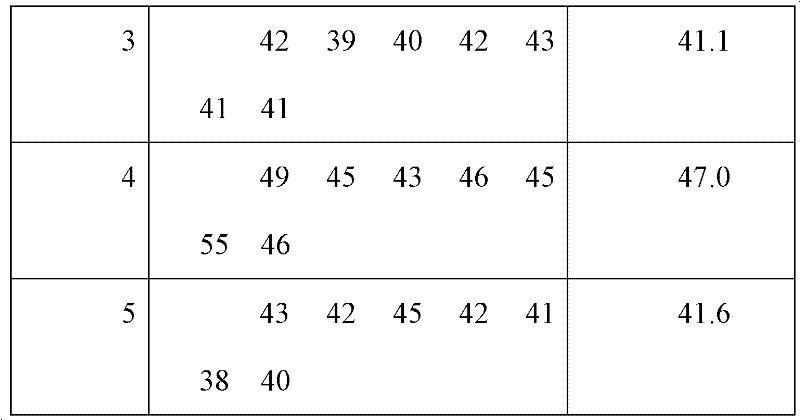
[0016] B. Contact resistance test

[0017] To measure the contact resistance between the missing bumps and the pads, select 5 chips at different positions on a 2-inch silicon wafer, with 7 bumps on each chip, and a total of 35 sets of data. The measurement data are shown in Table 2.

[0018] Table 2 Missing bump and pad contact resistance test data table

[0019]

[0020]

[0021] It can be seen from the data in the table that the...


PUM


Abstract

The invention discloses a process for making non-void high-reliability convex points in a wafer by vacuum brazing. A vacuum brazing furnace is used for welding, and the process comprises the following welding steps of: vacuumizing, introducing nitrogen, vacuumizing, preheating to the temperature of 150+/-10 DEG C in the nitrogen atmosphere, heating to the temperature of 210+/-10 DEG C, vacuumizing, performing water cooling, and back charging the nitrogen. By combining the process and a through printing method, small-size convex points with the diameter of 150 microns, the height of 100 microns and the distance of 250 microns are made. The process has the advantages of good consistency, simple flow, high production efficiency and low cost, and is suitable for large-batch production. The height tolerance of the through printed ball grid array (BGA) convex points is less than 3.0 microns, the linear consistency of the convex points is less than 5 microns, and the indexes of shearing strength, contact resistance and the like can meet the requirement of reliability.

Description

Technical field: [0001] The invention belongs to the field of microelectronic manufacturing technology; the invention relates to a technology for manufacturing high-reliability bumps on a wafer in combination with a solder paste missing printing technology. Background technique: [0002] At present, in the field of microelectronics, when the bump diameter is greater than 250 μm, solder paste printing technology or ball planting technology is usually used, and then solder paste or solder balls are melted by reflow soldering technology to form bumps on the wafer. Commonly used reflow soldering techniques include the following common methods: hot air heating, infrared heating, hot air + infrared heating, laser welding, etc. Regardless of whether heating is performed under a protective atmosphere, voids / holes or air bubbles in some solder joints after soldering cannot be avoided, and the reliability needs to be further improved. Invention content: [0003] The purpose of the ...

Claims


Application Information

Patent Timeline
Patent Type & Authority Applications(China)
IPC IPC(8): B23K1/008
Inventor 周海朱海峰姜伟刘帅洪
Owner NO 771 INST OF NO 9 RES INST CHINA AEROSPACE SCI & TECH
Why Eureka
Try Eureka