Technology of drop-out printing for manufacturing micron-sized salient point on wafer

A wafer and missing printing technology, used in printing, printing devices, semiconductor/solid-state device manufacturing, etc., can solve the problems of long time period and high relative cost, and achieve the effect of high production efficiency, low cost and simple process

Active Publication Date: 2013-08-07
郑州兴航科技有限公司
View PDF3 Cites 0 Cited by
  • Summary
  • Abstract
  • Description
  • Claims
  • Application Information

AI Technical Summary

Problems solved by technology

[0008] Common disadvantages: relatively high cost and long time period

Method used


Image

  • Technology of drop-out printing for manufacturing micron-sized salient point on wafer
  • Technology of drop-out printing for manufacturing micron-sized salient point on wafer
  • Technology of drop-out printing for manufacturing micron-sized salient point on wafer

Examples


Embodiment Construction

[0021] The present invention will be described in further detail below in conjunction with the accompanying drawings:

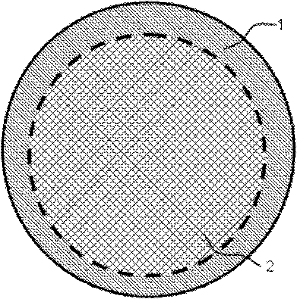
[0022] See figure 1 In the present invention, the above objectives are achieved by optimizing the leakage hole parameters of the stainless steel leakage plate, the thickness of the stainless steel leakage plate, the design leakage hole diameter, and the selection of solder paste parameters.

[0023] The process flow is as follows:

[0024] Drawing and plate making → making solder paste missing printing board → matching (solder paste missing printing) board → printing solder paste → inspection → welding → cleaning → inspection

[0025] 5.2 Parameters of solder paste missing printed board:

[0026] Solder paste missing plate material: stainless steel

[0027] Thickness of solder paste missing printing board: 0.1mm~0.15mm

[0028] Land size: 0.1mm~0.25mm

[0029] Leak hole size: 0.15mm~0.3mm

[0030] You can choose stainless steel as the material of the missing plate, and ch...


PUM


Abstract

The invention discloses a technology of paste printing for manufacturing a micron-sized salient point on a wafer. The method comprises the following steps that: a design is drawn and a plate is made; a welding paste printing plate is manufactured; a welding paste is printed on the welding paste printing plate; and then examination, welding, cleaning and detection are carried out successively. According to the invention, manufacture of a small-size salient point is realized, wherein a diameter of the salient point is 150 micrometers, a height of the salient point is 200 micrometers, and a gap is 250 micrometers. Besides, the technology provided in the invention has advantages of good consistency, simple flow, high production efficiency, and low costs, so that the technology is suitable forapplication on mass production. Moreover, a height tolerance of the printed BGA salient point is less thatn 3.0 microns and a linear consistency is less than 5 microns; and index like a shearing intensity and a contact resistor satisfies the requirement on reliability.

Description

Technical field: [0001] The present invention belongs to the field of microelectronic manufacturing technology; the present invention relates to a low-cost process method for producing 150 micron / 100 micron / 250 micron bumps on a wafer by missing printing. The 150 micron / 100 micron / 250 micron bumps respectively refer to the diameter, height and pitch of the bumps. Background technique: [0002] At present, in the field of microelectronics, solder paste omission technology or ball planting technology is used to make bumps. The capabilities are as follows: [0003] Among them, the ball planting method and the screen printing method can achieve a minimum bump diameter of 250μm and a minimum pitch of 400μm. They are mainly used in the production of Sn / Pb alloys, lead-free solders, and conductive paste bumps. The process is simple, low cost, and suitable For mass production. Internationally, the diameter of the bumps is usually 300μm~500μm, and the pitch is 500μm~800μm. The solder past...

Claims


Application Information

Patent Timeline
Patent Type & Authority Patents(China)
IPC IPC(8): H01L21/60B41M1/12B41M1/26
CPCH01L2224/11
Inventor 周海朱海峰姜伟刘帅洪
Owner 郑州兴航科技有限公司
Why Eureka
Try Eureka