Method for preventing grid electrode from damage in ion implantation process

A technology of ion implantation and process, which is applied in the direction of photosensitive material processing, electrical components, semiconductor/solid-state device manufacturing, etc., to avoid damage to the gate and improve the quality

Active Publication Date: 2012-03-14
SEMICONDUCTOR MANUFACTURING INTERNATIONAL (BEIJING) CORP +1
View PDF4 Cites 7 Cited by
  • Summary
  • Abstract
  • Description
  • Claims
  • Application Information

AI Technical Summary

Problems solved by technology

[0006] The technical problem to be solved by the present invention is to provide a method for preventing grid damage in the ion implantation process, so as to prevent the polymer formed inside the photoresist from being removed by the plasma during the photoresist removal process. During the step, it strongly impacts and interacts with the plasma, and a large amount of energy generated due to the hard surface barrier cannot be released and explodes, thus damaging the grid.

Method used


Image

  • Method for preventing grid electrode from damage in ion implantation process
  • Method for preventing grid electrode from damage in ion implantation process
  • Method for preventing grid electrode from damage in ion implantation process

Examples


Embodiment Construction

[0028] In order to make the content of the invention clearer and easier to understand, the content of the invention will be further described below in conjunction with the accompanying drawings. Of course, the invention is not limited to this specific embodiment, and general replacements known to those skilled in the art are also covered within the protection scope of the invention.

[0029] Secondly, the invention is described in detail with schematic diagrams. When describing the invention examples in detail, for the convenience of explanation, the schematic diagrams are not partially enlarged according to the general scale, which should not be used as a limitation to the invention.
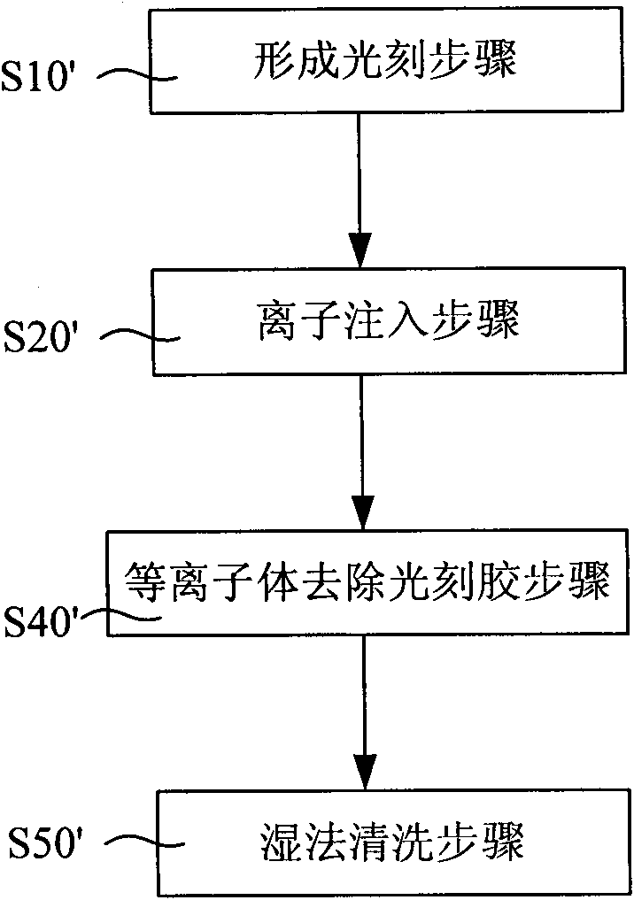
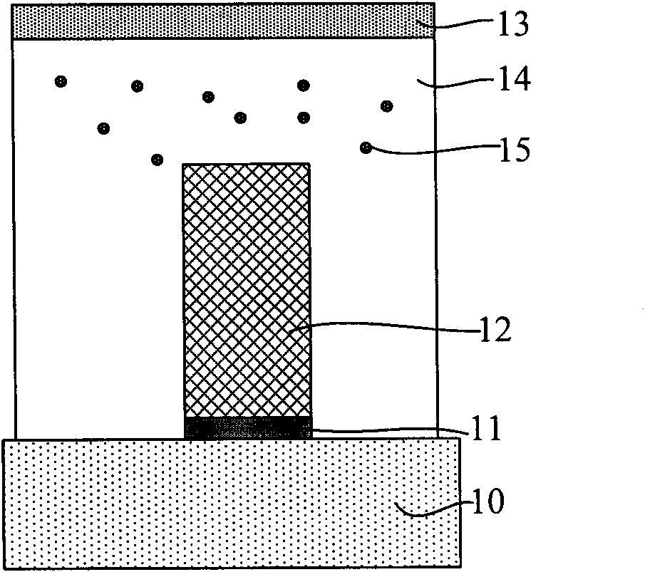
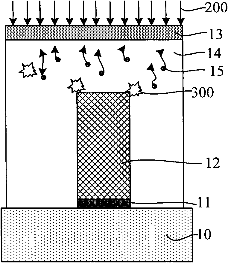
[0030] The core idea of ​​the invention is: by providing a method for preventing grid damage in the ion implantation process, a surface treatment step is added after the ion implantation step in the prior art and before the plasma photoresist removal step, including a rinsing step to remove the...


PUM


Abstract

The invention provides a method for preventing a grid electrode from damage in an ion implantation process. The ion implantation process comprises a photoresist forming step, an ion implantation step and a plasma photoresist removal step. A surface treatment step is also comprised between the ion implantation step and the plasma photoresist removal step. The surface treatment step comprises a washing step, a baking step and a cooling step. In the method for preventing the grid electrode from the damage in the ion implantation process, the surface treatment step is added between the ion implantation step and the plasma photoresist removal step so as to remove a hard surface layer formed on the surface of a photoresist and a polymer formed in the photoresist in the ion implantation step, and further, the phenomenon that a plasma and the polymer act with each other to explode in the plasma photoresist removal step is avoided, thereby, the condition that the grid electrode is damaged is avoided, and the quality of a device is improved.

Description

technical field [0001] The invention relates to the technical field of semiconductor manufacturing, in particular to a method for preventing grid damage in an ion implantation process. Background technique [0002] With the rapid development of semiconductor manufacturing technology, in order to achieve faster computing speed, larger data storage capacity and more functions of semiconductor devices, semiconductor wafers are developing towards higher component density and high integration. The characteristics of CMOS devices Dimensions have gone down to the deep sub-micron level and even smaller, gate lengths are getting thinner and shorter than ever. In the prior art, for micro-subnanometer CMOS devices such as 43nm process, the density of transistors is greatly increased, and it becomes a trend to perform high-dose ion implantation in the source region and the drain region. [0003] After the gate oxide layer and the gate are formed on the semiconductor substrate, the NMOS...

Claims


Application Information

Patent Timeline
Patent Type & Authority Applications(China)
IPC IPC(8): H01L21/265G03F7/42G03F7/38
Inventor 张轲潘贤俊车永强
Owner SEMICONDUCTOR MANUFACTURING INTERNATIONAL (BEIJING) CORP
Why Eureka
Try Eureka