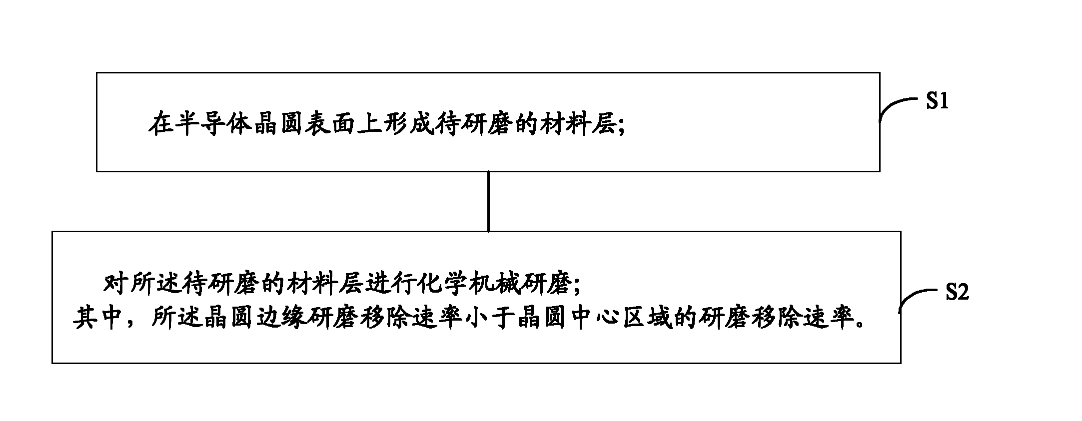
Method for preventing low yield of wafer edge device
A wafer and yield technology, which is applied in semiconductor/solid-state device manufacturing, electrical components, grinding devices, etc., can solve the problems of poor edge performance and low yield of wafer edge devices, so as to improve grinding uniformity and reduce Grinding removal rate, the effect of improving production yield
- Summary
- Abstract
- Description
- Claims
- Application Information
AI Technical Summary
Problems solved by technology
Method used
Image

Examples
Embodiment Construction
[0037] In the following description, numerous specific details are set forth in order to provide a thorough understanding of the present invention. However, the present invention can be implemented in many other ways different from those described here, and those skilled in the art can make similar extensions without violating the connotation of the present invention, so the present invention is not limited by the specific embodiments disclosed below.
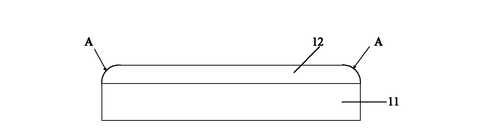
[0038] In the manufacturing process of semiconductor devices, there are often situations where the yield rate of wafer edge devices is reduced. The inventors have found through analysis that the main reason for the low yield rate of wafer edge devices is that the wafer edge will be excessively ground after the planarization process. In turn, a short circuit occurs, resulting in low yield of wafer edge devices. Detailed description will be given below.
[0039] In the process of forming metal interconnections, photoresist is us...
PUM
 Abstract
Description
Claims
Application Information
 - Generate Ideas
- Intellectual Property
- Life Sciences
- Materials
- Tech Scout
- Unparalleled Data Quality
- Higher Quality Content
- 60% Fewer Hallucinations
Browse by: Latest US Patents, China's latest patents, Technical Efficacy Thesaurus, Application Domain, Technology Topic, Popular Technical Reports.
© 2025 PatSnap. All rights reserved.Legal|Privacy policy|Modern Slavery Act Transparency Statement|Sitemap|About US| Contact US: help@patsnap.com