Supercharge Your Innovation With Domain-Expert AI Agents!

Method for preparing semiconductor structure for detection by transmission electron microscope, and semiconductor structure

An electron microscope and semiconductor technology, applied in semiconductor/solid-state device manufacturing, semiconductor devices, semiconductor/solid-state device components, etc., can solve problems such as through-hole deformation and inability to clearly obtain transmission electron microscope detection image data

Active Publication Date: 2014-03-19
SEMICON MFG INT (SHANGHAI) CORP +1
View PDF5 Cites 0 Cited by
  • Summary
  • Abstract
  • Description
  • Claims
  • Application Information

AI Technical Summary

Problems solved by technology

[0010] In order to solve the problem of deformation of the through hole and the ensuing inability to clearly obtain the image data of the transmission electron microscope when the barrier layer and the seed layer are covered by the transmission electron microscope in the prior art, the present invention discloses a method for A method of preparing a semiconductor structure detected by a transmission electron microscope, the method comprising the steps of: providing a front-end device on which a dielectric material layer is formed; depositing a barrier layer on the dielectric material layer; Depositing a first seed layer on the barrier layer; setting an interface layer on the first seed layer; depositing a second seed layer on the interface layer; setting a filling layer on the second seed layer

Method used


Image

  • Method for preparing semiconductor structure for detection by transmission electron microscope, and semiconductor structure
  • Method for preparing semiconductor structure for detection by transmission electron microscope, and semiconductor structure
  • Method for preparing semiconductor structure for detection by transmission electron microscope, and semiconductor structure

Examples


Embodiment Construction

[0038] In the following description, numerous specific details are given in order to provide a more thorough understanding of the present invention. It will be apparent, however, to one skilled in the art that the present invention may be practiced without one or more of these details. In other examples, some technical features known in the art are not described in order to avoid confusion with the present invention.

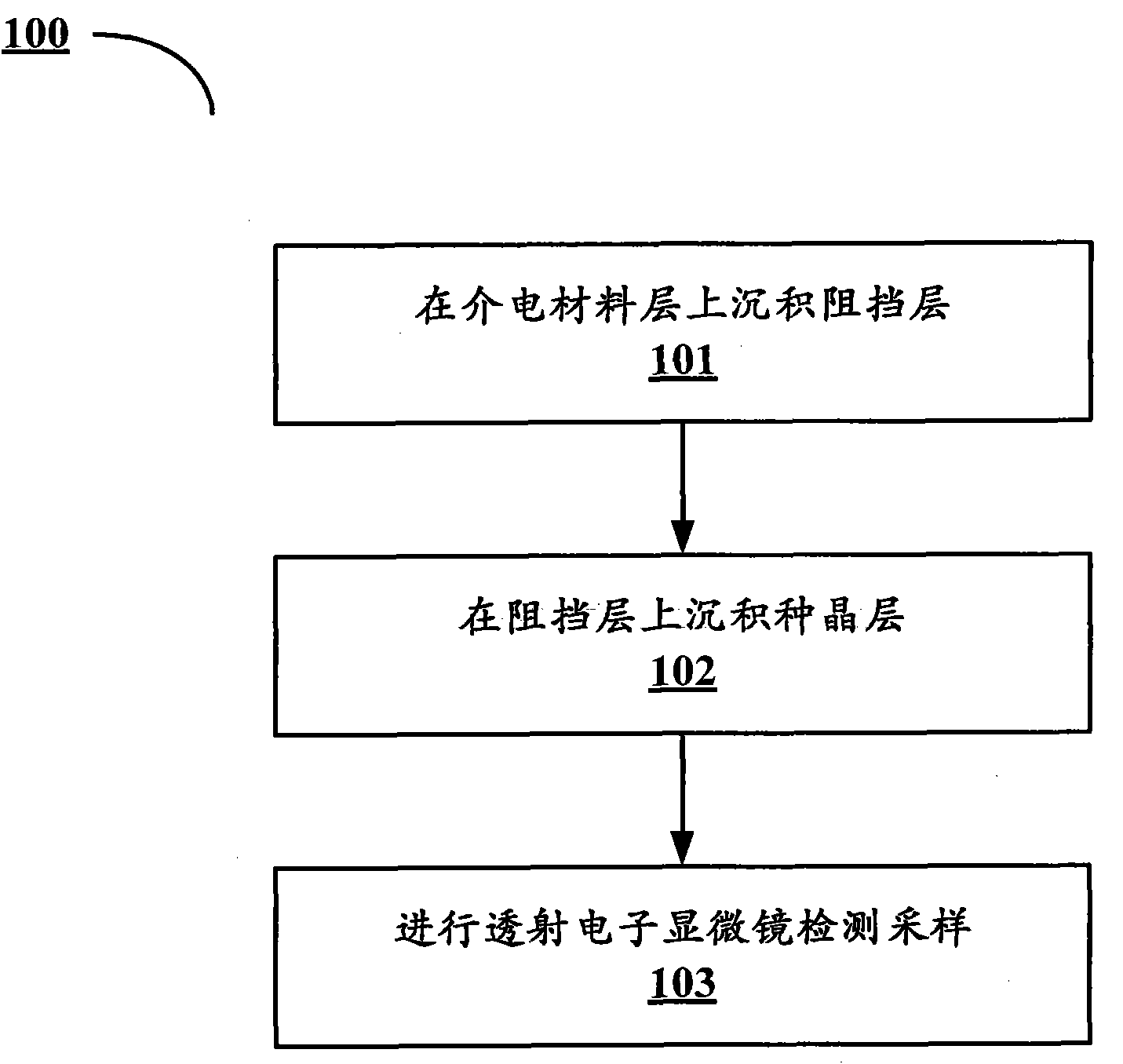
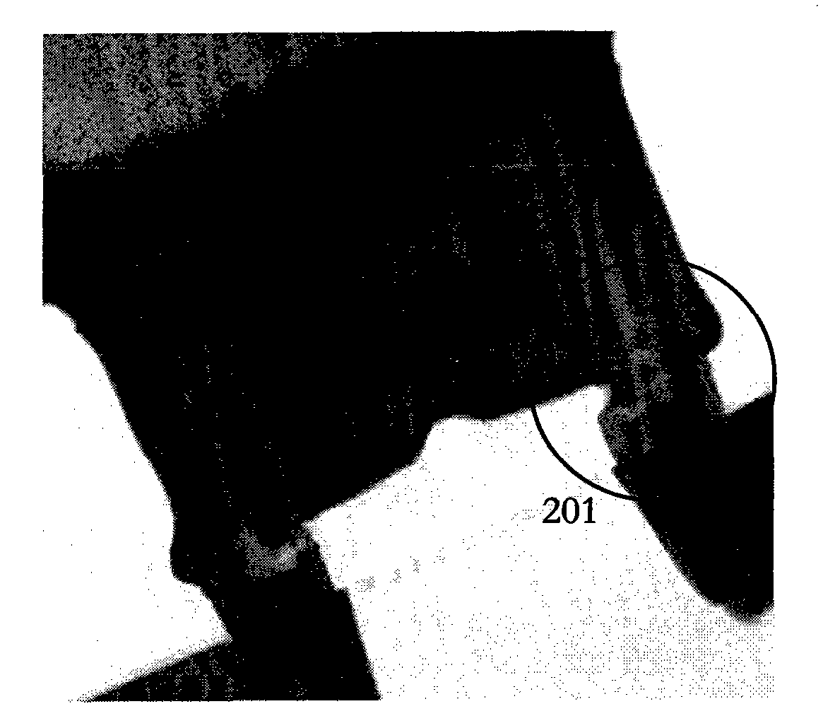
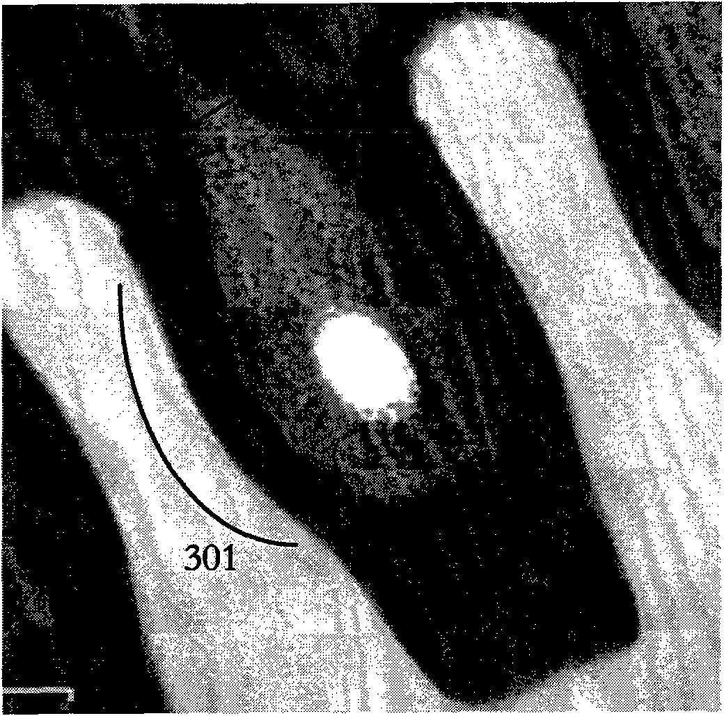
[0039] In order to thoroughly understand the present invention, detailed steps and structures will be proposed in the following description, so as to explain how the present invention solves the problem that the prior art cannot ensure that the via hole is not detected when the step coverage of the barrier layer and the seed layer is inspected by transmission electron microscopy. The problem of being damaged and deformed. Obviously, the practice of the invention is not limited to specific details familiar to those skilled in the semiconductor arts. Preferred e...


PUM


Abstract

The invention discloses a method for preparing a semiconductor structure for the detection by a transmission electron microscope, which comprises the steps of: providing a front-end device, and forming a dielectric material layer on the front-end device; depositing a barrier layer on the dielectric material layer; depositing a first seed crystal layer on the barrier layer; setting an interface layer on the first seed crystal layer; depositing a second seed crystal layer on the interface layer; and setting a filling layer on the second seed crystal layer. The invention further discloses a semiconductor structure for the detection by the transmission electron microscope. The method and the structure can be conveniently applicable to a copper interconnection technology when a semiconductor is manufactured, step coverage which is performed to the barrier layer and the seed crystal layers is detected by the transmission electron microscope, a through hole cannot be deformed when the transmission electron microscope is used for sampling, and the detecting image of the transmission electron microscope, which shows the step coverage of the barrier layer and the seed crystal layers, can be further clearly obtained.

Description

technical field [0001] The invention relates to the technical field of semiconductor manufacturing, in particular to a method and structure for detecting step coverage of a barrier layer and a seed crystal layer in a semiconductor structure by a transmission electron microscope (TEM). Background technique [0002] With the development of VLSI technology, semiconductor technology has now entered the era of ultra-deep submicron. At newer process levels, especially at technology nodes of 90nm or below, the major signal delays come from the parts of the interconnecting circuits. Aluminum, which is mainly used as a metal interconnection material in traditional semiconductor processes, has been limited in signal delay. Therefore, a new material has been found to meet the requirements for resistance, and this material is copper. Simply put, copper technology refers to a series of semiconductor manufacturing processes that use copper as a metal interconnect material. Integrating ...

Claims


Application Information

Patent Timeline
Patent Type & Authority Patents(China)
IPC IPC(8): H01L21/768H01L23/532
Inventor 何伟业庞凌华王玉科聂佳相杨瑞鹏
Owner SEMICON MFG INT (SHANGHAI) CORP
Features
  • R&D
  • Intellectual Property
  • Life Sciences
  • Materials
  • Tech Scout
  • Unparalleled Data Quality
  • Higher Quality Content
  • 60% Fewer Hallucinations
Learn More