Silicone tunable optical filter and making method thereof

A filter and bulk silicon technology, applied in the field of bulk silicon tunable optical filters and fabrication, can solve problems such as high stress control requirements, deformed transmitted light signals, residual stress, etc., achieve good optical performance, simple processing technology, The effect of high structural reliability

Active Publication Date: 2011-09-28
SHANGHAI INST OF MICROSYSTEM & INFORMATION TECH CHINESE ACAD OF SCI
View PDF6 Cites 22 Cited by
  • Summary
  • Abstract
  • Description
  • Claims
  • Application Information

AI Technical Summary

Problems solved by technology

The disadvantages of adopting this scheme are: 1) The stress control requirements for thin-film silicon materials are high, and residual stress is likely to be caused when making silicon thin films, thereby causing deformation on the surface of silicon thin-film materials and degrading the transmitted light signal; 2) growing The thickness of the polysilicon film is usually several microns, and it is difficult to grow thicker films; 3) The surface optical quality of the polysilicon film is poor, such as roughness, which is difficult to control and affects the optical performance of the F-P interference cavity; 4) The film material requires stress control. It is also impossible to make a large-area mirror, resulting in the final optical coupling that can only be packaged with a small-spot fiber optic lens, resulting in an increase in the overall cost of the device and a decrease in reliability

Method used


Image

  • Silicone tunable optical filter and making method thereof
  • Silicone tunable optical filter and making method thereof
  • Silicone tunable optical filter and making method thereof

Examples


Embodiment Construction

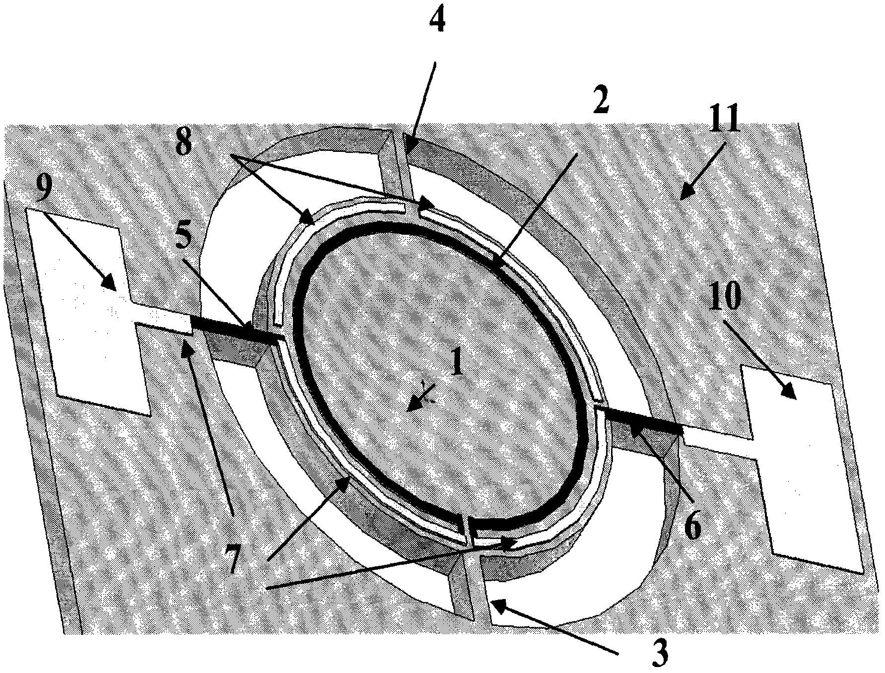
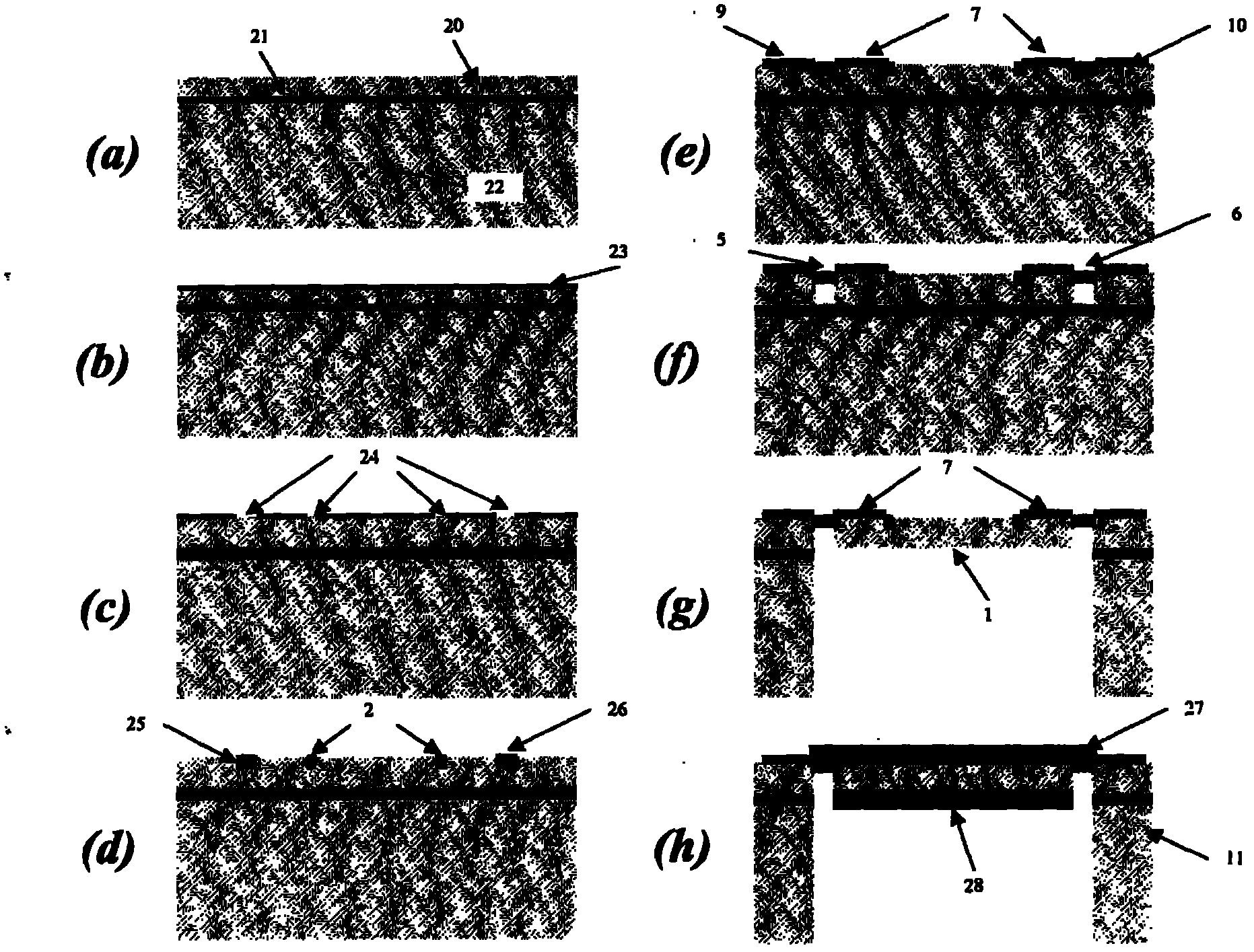
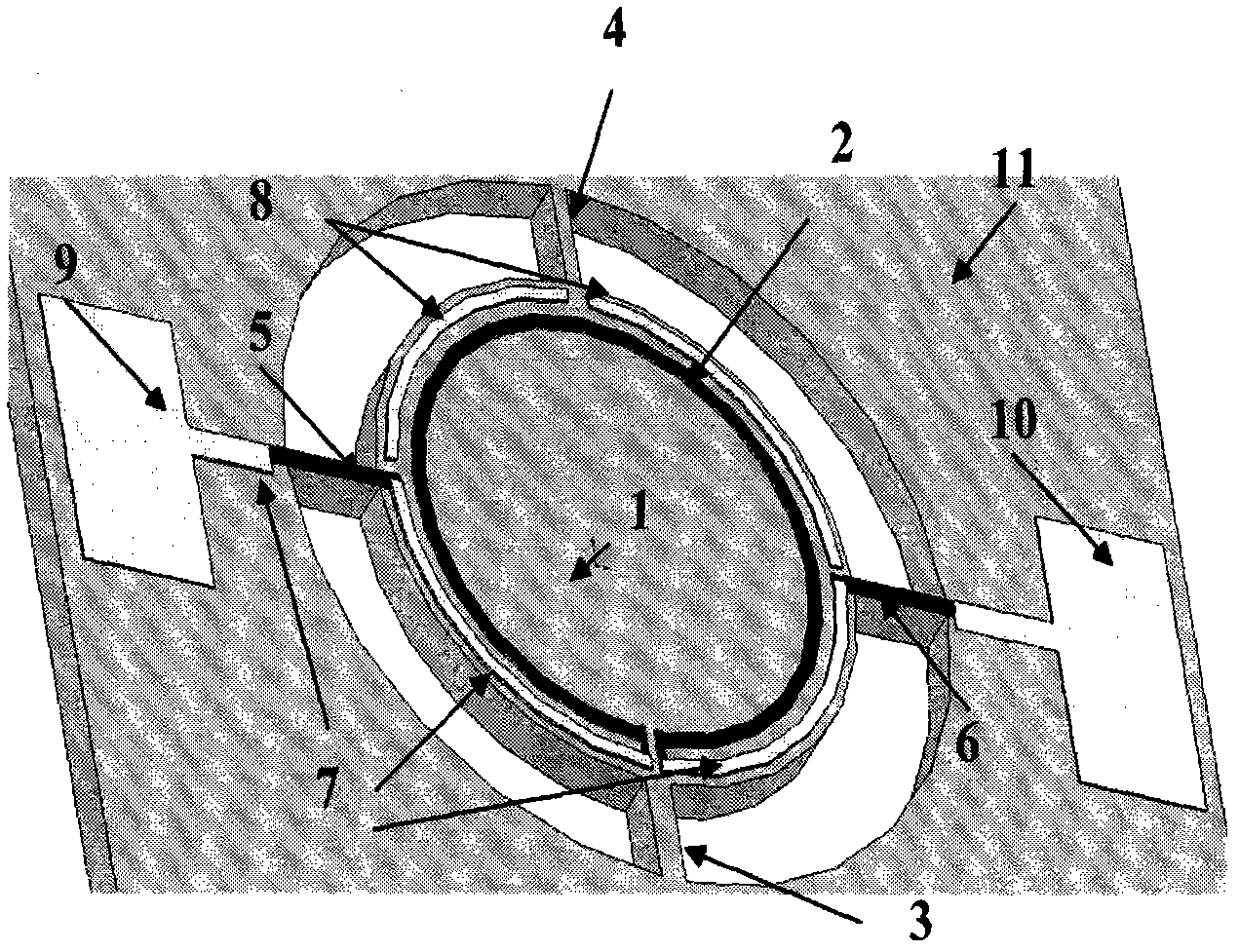
[0022] A bulk silicon tunable optical filter proposed by the present invention consists of a bulk silicon tuning cavity 1, a highly doped bulk silicon resistance heater 2, a lower cantilever beam 3, an upper cantilever beam 4, and a left cantilever beam 5 with a highly doped surface 1. A right cantilever beam 6 with a highly doped surface, a metal wire 7, a stress balance metal wire 8, a left lead area 9, a right lead area 10, and a supporting silicon substrate 11. Its structure is as figure 1 shown. The bulk silicon tuning cavity 1 is entirely composed of a single crystal silicon device layer of a high-resistivity SOI silicon wafer, and has good parallelism and surface optical quality. At the same time, the bulk silicon tuning cavity 1 can produce a large optical aperture. The highly doped bulk silicon resistance heater 2 is made of high-concentration semiconductor doping material, which can produce the heating resistance value required by the design, and use it to uniforml...


PUM

PropertyMeasurementUnit
electrical resistivityaaaaaaaaaa
thicknessaaaaaaaaaa
thicknessaaaaaaaaaa

Abstract

The invention provides a silicone tunable optical filter, comprising a silicone tuning cavity, a highly-doped silicone resistance heater, a lower cantilever beam, an upper cantilever beam, a left surface highly-doped cantilever beam, a right highly surface doped cantilever beam, a metal lead, a stress balancing metal lead, a left lead region, a right lead region and an SOI (Silicon-on-Insulator) supporting silicon substrate 11. The silicone tunable optical filter is obtained by using an SOI wafer with high resistance and a silicone machining process. A making method provided by the invention comprises the following steps of: (a) making a highly doped region on the surface of an SOI wafer device layer; (b) sputtering metal on the surface of the wafer device layer and making a metal structure; (c) making the silicone tuning cavity and each cantilever beam structure on the surface of the wafer device layer; (d) releasing the silicone tuning cavity and the cantilever beam structure from asubstrate layer of the lower surface of the silicon wafer; and (e) making high reflective films on the upper and lower surfaces of the silicone tuning cavity to form an optical F-P interference cavity body. The made filter has the advantages of very good optical performance, simple making process and high structural reliability.

Description

technical field [0001] The invention relates to a tunable optical device and a manufacturing method used in the fields of optical fiber communication, optical fiber sensing and fiber lasers, in particular to a bulk silicon tunable optical filter and a manufacturing method. The invention belongs to the field of tunable optical filter. Background technique [0002] With the rapid development of optical communication, Dense Wavelength Division Multiplexing (DWDM) has become the mainstream of optical communication network. The core device is the wavelength multiplexer / demultiplexer. One of the main applications of tunable filters is to form various demultiplexers, which can separate the optical signals multiplexed together. Tunable filters can also constitute key devices in the new generation of all-optical networks, namely optical add-drop multiplexers (ROADMs) and optical performance monitors (OPMs). In the field of optical fiber sensors, the wavelength resolution of fiber g...

Claims


Application Information

Patent Timeline
Patent Type & Authority Applications(China)
IPC IPC(8): G02F1/21
Inventor 李四华吴亚明
Owner SHANGHAI INST OF MICROSYSTEM & INFORMATION TECH CHINESE ACAD OF SCI
Why Eureka
Try Eureka