Signal wiring structure in GOA (gate driver on array) circuit of liquid crystal display

A liquid crystal display and line structure technology, applied in static indicators, instruments, nonlinear optics, etc., can solve problems such as abnormal image display, uneven signal bus impedance, affecting the input and output of GOA circuits, etc., to achieve uniform impedance values, Improve the image display quality, the effect of input signal and output signal stability

Inactive Publication Date: 2012-03-28
AU OPTRONICS CORP
View PDF0 Cites 23 Cited by
  • Summary
  • Abstract
  • Description
  • Claims
  • Application Information

AI Technical Summary

Problems solved by technology

In this way, the impedance on the signal bus CK1~CK6 will be uneven, which will affect the input and output of each stage of GOA circuit, resulting in abnormal image display

Method used


Image

  • Signal wiring structure in GOA (gate driver on array) circuit of liquid crystal display
  • Signal wiring structure in GOA (gate driver on array) circuit of liquid crystal display

Examples


Embodiment Construction

[0021] In order to make the technical content disclosed in this application more detailed and complete, reference may be made to the drawings and the following various specific embodiments of the present invention, and the same symbols in the drawings represent the same or similar components. However, those skilled in the art should understand that the examples provided below are not intended to limit the scope of the present invention. In addition, the drawings are only for schematic illustration and are not drawn according to their original scale.

[0022] The specific implementation manners of various aspects of the present invention will be further described in detail below with reference to the accompanying drawings.

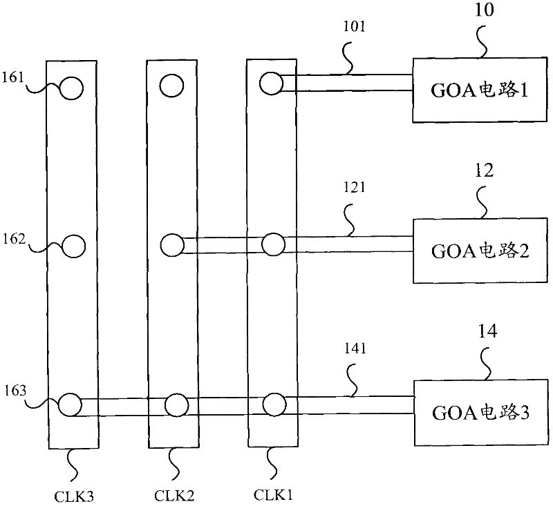
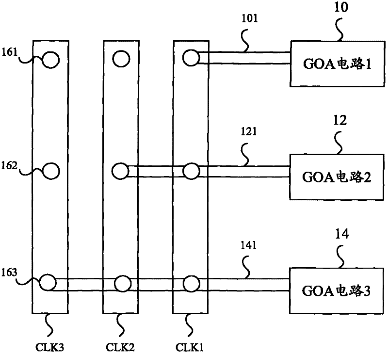
[0023] figure 1 According to one aspect of the present invention, it is a block diagram showing a signal wiring structure in a GOA (Gate driver On Array, array substrate row driver) circuit for a liquid crystal display. refer to figure 1 , the signal rou...


PUM


Abstract

The invention provides a signal wiring structure in a GOA (gate driver on array) circuit of a liquid crystal display. The structure comprises a plurality of first metal layers, an insulating layer and a plurality of second metal layers, wherein each first metal layer is provided with a control signal wire; the insulating layer is formed under the first metal layers; the plurality of second metal layers are formed under the insulating layer, and the control signal wire on each first metal layer is electrically connected with the corresponding second metal layer through a plurality of through holes; and the number of the through holes formed on the control signal wire on each first metal layer is the same. According to the signal wiring structure, the control signal wire on each first metal layer is electrically connected with the second metal layer through a plurality of through holes, and the number of the through holes formed on the control signal wire on each first metal layer is the same, so that the impedance values on all control signal wires are uniform, and input and output signals of each stage of the GOA circuit are stable, and the image display quality is improved.

Description

technical field [0001] The invention relates to a GOA circuit of a liquid crystal display, in particular to a signal wiring structure for the GOA circuit. Background technique [0002] Currently, in an active matrix liquid crystal display (AMLCD, Active Matrix Liquid Crystal Display), each pixel has a thin film transistor (TFT, Thin Film Transistor), the gate of which is electrically connected to the horizontal scanning line, and the drain is electrically The source is electrically connected to the data line in the vertical direction, and the source is electrically connected to the pixel electrode. If enough positive voltage is applied to a scanning line in the horizontal direction, all the TFTs on the scanning line will be turned on. At this time, the pixel electrode corresponding to the scanning line will be connected to the data line in the vertical direction, and the data line will be The video signal voltage is written into the pixel, so as to control the light transmi...

Claims


Application Information

Patent Timeline
IPC IPC(8): G02F1/1362G02F1/133
Inventor 张竣桓刘俊欣林坤岳林雅婷
Owner AU OPTRONICS CORP
Why Eureka
Try Eureka