Wire-planting circuit board, its processing method and processing equipment

A processing method and circuit board technology, applied in printed circuit, printed circuit manufacturing, printed circuit components, etc., can solve the problems of uneven impedance, not high-frequency high-speed materials, large microstrip lines, etc., and achieve uniform physical properties , Reliable mechanical performance, good electromagnetic performance

Active Publication Date: 2022-03-04
宁波甬强科技有限公司
View PDF6 Cites 0 Cited by
  • Summary
  • Abstract
  • Description
  • Claims
  • Application Information

AI Technical Summary

Problems solved by technology

Wiring by etching, the texture of the glass cloth cannot be well known, the wiring is relatively random, and the texture will affect the electrical performance of the stripline, such as uneven impedance, etc.
[0008] Third, the etched microstrip line has a large tolerance, the shape of the cross section cannot be optimized, and only copper can be used, etc., which greatly affects the transmission of high-speed signals.
[0009] Fourth, the main processing metal of CCL is copper, which is not the best high-frequency and high-speed material
[0010] To sum up, the existing printed circuit manufacturing method and the structure of the printed circuit board cannot meet the requirements of high-speed signal transmission.

Method used


Image

  • Wire-planting circuit board, its processing method and processing equipment
  • Wire-planting circuit board, its processing method and processing equipment
  • Wire-planting circuit board, its processing method and processing equipment

Examples


Embodiment Construction

[0049] Specific embodiments of the present invention will be described in detail below in conjunction with the accompanying drawings.

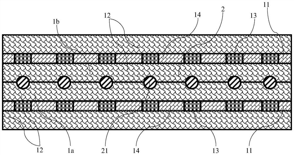
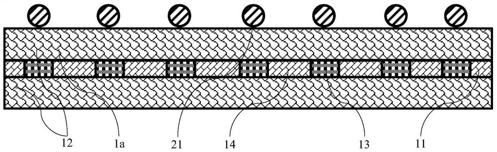
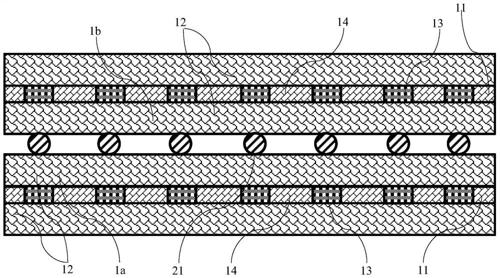
[0050] refer to figure 1 As shown in the figure, a schematic cross-sectional view of an embodiment of the wire-planting circuit board provided by the present invention is shown, and unnecessary structural features are canceled. Of course, it is not used to limit the weaving process of glass fiber cloth, but is only used to illustrate the composition of the planting involved in the present invention. The basic structural relationship between the various components of the circuit board is shown. The wire-planted circuit board provided by the present invention includes: prepreg layers 1a, 1b, the prepreg layers include a reinforcing part 11 and a bonding part 12, and the reinforcing part 11 has lines. figure 1 As shown in , the texture is formed by warp threads 13 and weft threads 14. The wire layer 2 , the wire layer 2 is implanted at the bond...


PUM


Abstract

A wire planting circuit board, comprising: a prepreg layer, the prepreg layer includes a reinforcing part and a bonding part, the reinforcing part has textures; a wire layer, the wire layer is implanted in the bonding part, and the wire layer is arranged according to the texture. A processing method for a wire planting circuit board, comprising: directly arranging wires on a prepreg according to set wire layout requirements. A processing device for wire planting circuit boards, comprising: a wiring machine, the wiring machine is used to arrange the wires on the bonding part of the prepreg according to the pattern of the reinforcing part of the prepreg. Accordingly, the technical effect that the present invention can achieve is that the roughness of the wire layer and its physical properties in the bonding part are uniform, thus, the electrical properties of the wire layer are improved (uniform impedance, low loss, good electromagnetic performance, etc.) Moreover, the mechanical performance is reliable, and it is suitable for transmitting high-speed and high-frequency electrical signals. Moreover, according to the processing method provided by the present invention, the aforementioned wire-planted circuit board can be manufactured by using the processing equipment provided by the present invention.

Description

technical field [0001] The invention relates to the field of design and production of wire-planted circuit boards, in particular to a wire-planted circuit board, a processing method for a wire-planted circuit board and processing equipment for a wire-planted circuit board. Background technique [0002] The manufacturing method of the printed circuit board in the prior art is: briefly summarized as forming the required stripline or microstrip line on the copper clad board by etching for signal transmission. [0003] In the 4G era, the PCB single-channel signal transmission rate has been increased from 10Gbps to 25Gbps, and it is expected to further increase to more than 50Gbps in the 5G era. The high-speed / high-frequency signal means that the signal transmission is more and more concentrated on the "surface layer" of the wire (called the skin effect). When the frequency reaches 1GHz, the transmission thickness of the signal on the surface of the wire is only 2.1μm. If the sur...

Claims


Application Information

Patent Timeline
Patent Type & Authority Patents(China)
IPC IPC(8): H05K1/02H05K3/00
CPCH05K1/0296H05K3/0002
Inventor 张玮洪丹红
Owner 宁波甬强科技有限公司
Why Eureka
Try Eureka