Method for fabricating a strained semiconductor-on-insulator substrate

a technology of semiconductors and substrates, applied in semiconductor/solid-state device manufacturing, basic electric elements, electric devices, etc., can solve the problems of chemical-mechanical polishing not being compatible, loss of effectiveness in transferring strain from the layer to the transferred monocrystalline silicon layer, and inability to use conventional thermal smoothing techniques on ssoi substrates containing silicon-germanium layers. achieve uniformity and roughness

Active Publication Date: 2021-03-23
SOITEC SA
View PDF8 Cites 4 Cited by
  • Summary
  • Abstract
  • Description
  • Claims
  • Application Information

AI Technical Summary

Benefits of technology

[0020]One aim of the present disclosure is to design a method for fabricating a strained semiconductor-on-insulator substrate that allows the uniformity and roughness required for the strained semiconductor layer to be obtained without a loss of effectiveness in transferring strain.
[0031]The use of a donor substrate comprising multiple layers of different chemical compositions that may be selectively etched in succession makes it possible to avoid having to use annealing for the purpose of smoothing in order to obtain the uniformity and roughness desired for the strained semiconductor layer of the final substrate.

Problems solved by technology

Conventional thermal smoothing techniques cannot be used on an sSOI substrate containing a silicon-germanium layer.
Specifically, the heat treatment used would cause a portion of the germanium to diffuse out of the silicon-germanium layer, resulting in a loss of effectiveness in transferring strain from the layer to the transferred monocrystalline silicon layer.
Furthermore, chemical-mechanical polishing is not compatible given the current state of the art on the subject with the desired uniformity of thickness.

Method used


Image

  • Method for fabricating a strained semiconductor-on-insulator substrate
  • Method for fabricating a strained semiconductor-on-insulator substrate
  • Method for fabricating a strained semiconductor-on-insulator substrate

Examples


Embodiment Construction

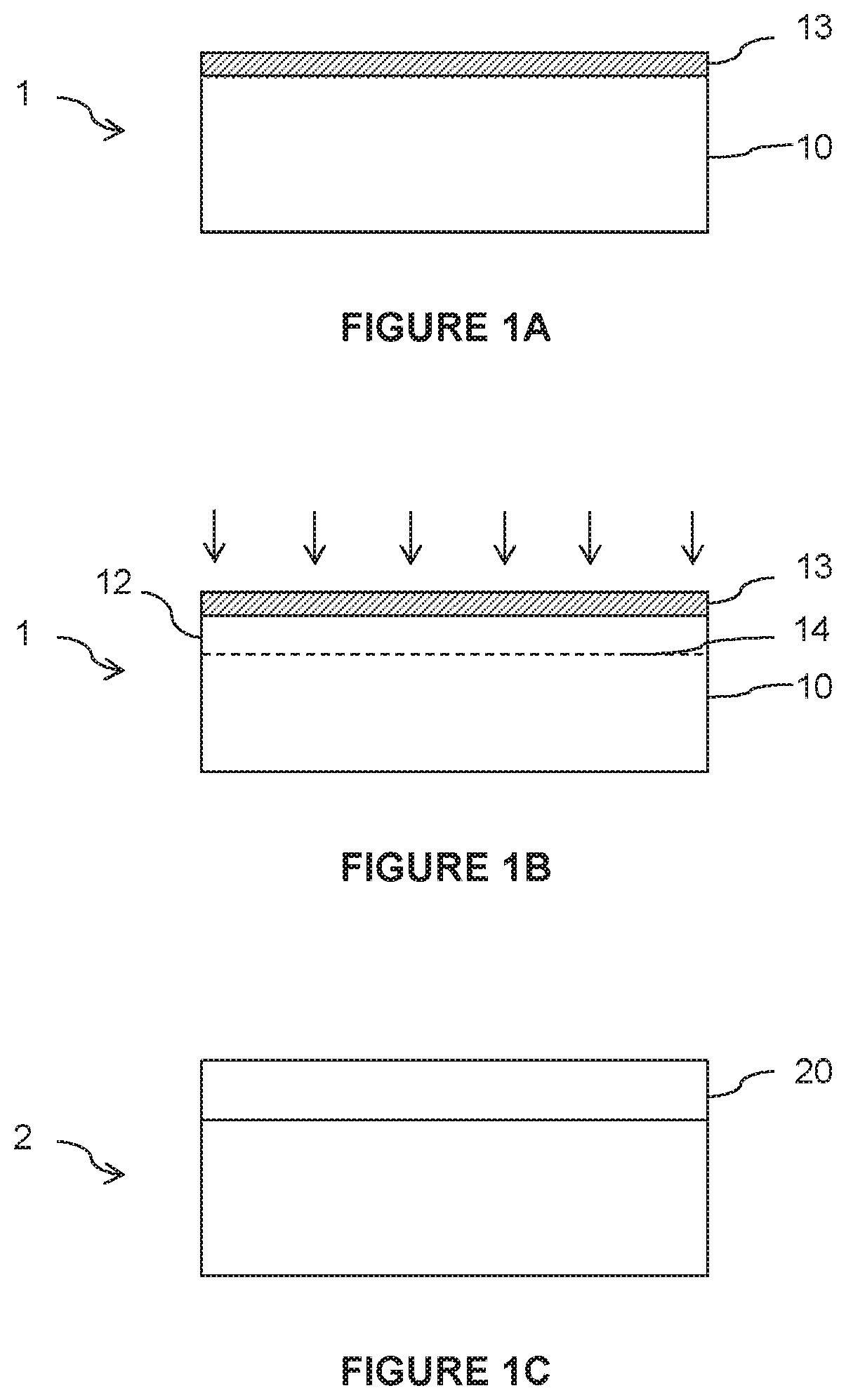
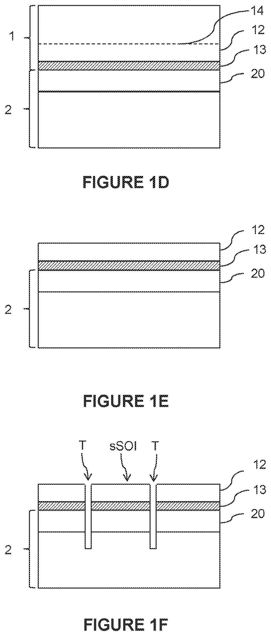
[0055]A donor substrate is provided that comprises at least one monocrystalline semiconductor layer that is intended to form the strained layer of the sSOI substrate.

[0056]The donor substrate is a composite substrate, i.e., it consists of at least two layers of different materials, including the monocrystalline semiconductor layer, which is arranged on the surface of the substrate.

[0057]More specifically, the donor substrate comprises, in succession, a monocrystalline carrier substrate, an intermediate layer and the monocrystalline semiconductor layer, the intermediate layer forming an etch-stop layer with respect to the material of the carrier substrate and to the material of the monocrystalline semiconductor layer. To achieve this, the intermediate layer is made of a material having a chemical composition that differs from that of the carrier substrate and of the monocrystalline semiconductor layer, the choice of materials potentially being made according to the nature of the etch...


PUM

PropertyMeasurementUnit
thicknessaaaaaaaaaa
thicknessaaaaaaaaaa
thicknessaaaaaaaaaa

Abstract

A method for fabricating a strained semiconductor-on-insulator substrate comprises bonding a donor substrate to a receiving substrate with a dielectric layer at the interface. The donor substrate comprises a monocrystalline carrier substrate, an intermediate etch-stop layer, and a monocrystalline semiconductor layer. The monocrystalline semiconductor layer is transferred from the donor substrate to the receiving substrate. Trench isolations are formed to cut a portion from a layer stack including the transferred monocrystalline semiconductor layer, the dielectric layer, and the strained semiconductor material layer. The cutting operation results in relaxation of strain in the strained semiconductor material, and in application of strain to the transferred monocrystalline semiconductor layer. After transferring the monocrystalline semiconductor layer and before the cutting operation, a portion of the carrier substrate is selectively etched with respect to the intermediate layer, and the intermediate layer is selectively etched with respect to the monocrystalline semiconductor layer.

Description

CROSS-REFERENCE TO RELATED APPLICATIONS[0001]This application is a national phase entry under 35 U.S.C. § 371 of International Patent Application PCT / EP2017 / 061793, filed May 17, 2017, designating the United States of America and published in English as International Patent Publication WO 2017 / 198687 A1 on Nov. 23, 2017, which claims the benefit under Article 8 of the Patent Cooperation Treaty to French Patent Application Serial No. 1654369, filed May 17, 2016.TECHNICAL FIELD[0002]The present disclosure relates to a method for fabricating a strained semiconductor-on-insulator substrate.BACKGROUND[0003]For digital applications, in particular, for technological nodes beyond the 22 nm node, materials with enhanced charge carrier mobility are sought.[0004]Among these materials, FDSOI (acronym for fully depleted silicon-on-insulator) substrates feature a very thin (i.e., typically less than 50 nm thick) layer of silicon on a buried electrically insulating layer, the silicon layer potenti...

Claims


Application Information

Patent Timeline
Patent Type & Authority Patents(United States)
IPC IPC(8): H01L21/00H01L21/762
CPCH01L21/76275H01L21/76254
Inventor SCHWARZENBACH, WALTERCHABANNE, GUILLAUMEDAVAL, NICOLAS
Owner SOITEC SA
Why Eureka
Try Eureka