Single event upset resistant settable and resettable scan structure D flip-flop

An anti-single-event, trigger technology, applied in the direction of electrical pulse generator circuit, reliability improvement modification, pulse generation, etc., can solve the problem of low anti-single-event flipping ability.

Active Publication Date: 2012-03-28
NAT UNIV OF DEFENSE TECH
View PDF6 Cites 8 Cited by
  • Summary
  • Abstract
  • Description
  • Claims
  • Application Information

AI Technical Summary

Problems solved by technology

[0009] The technical problem to be solved by the present invention is to propose a settable and resettable anti-single event flip-flop scanning structure D flip-flop that has low anti-single event flip-flop ability. Structural D flip-flop, which can work well under single-event bombardment with higher LET values ​​without single-event flipping

Method used


Image

  • Single event upset resistant settable and resettable scan structure D flip-flop
  • Single event upset resistant settable and resettable scan structure D flip-flop
  • Single event upset resistant settable and resettable scan structure D flip-flop

Examples


Embodiment Construction

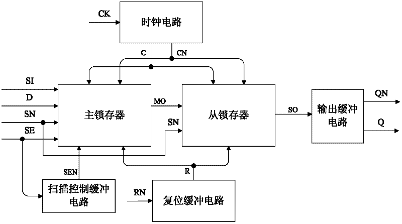
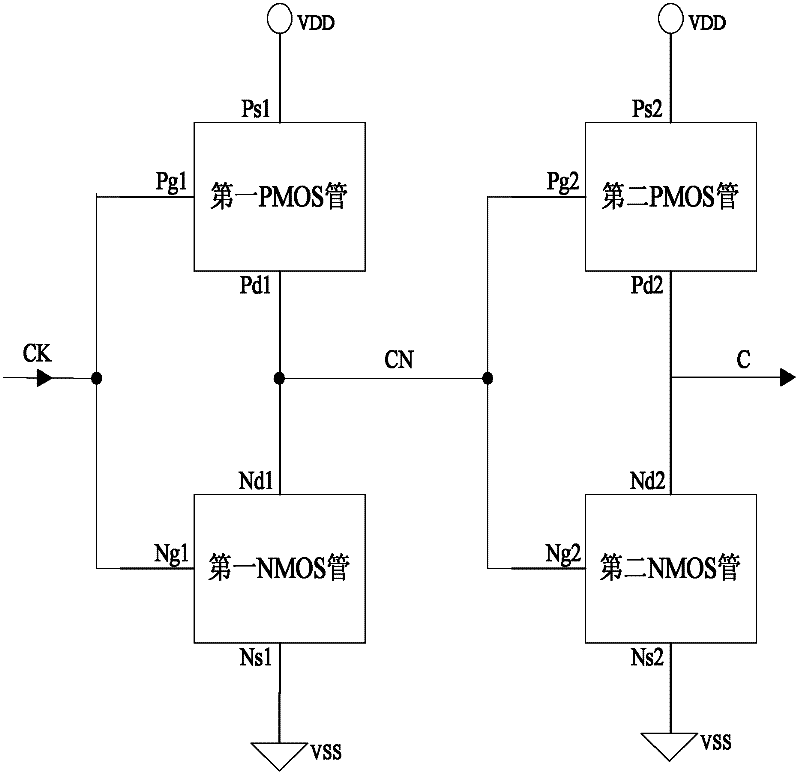
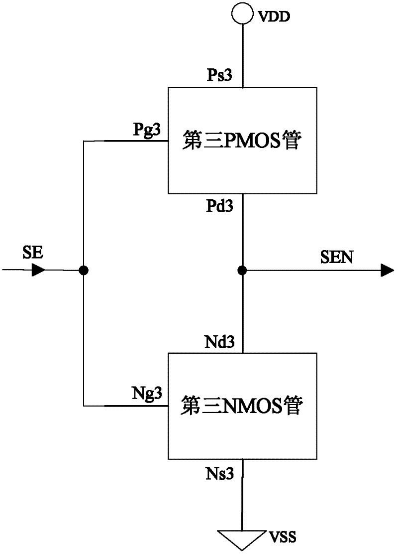
[0034] figure 1 It is a schematic diagram of the logic structure of the anti-single event reversal D flip-flop of the scanning structure which can be set and reset in the present invention. The present invention consists of a clock circuit (such as figure 2 shown), scan control buffer circuit (such as image 3 shown), reset buffer circuit (such as Figure 4 shown), the master latch (as Figure 5 shown), slave latches (such as Image 6 shown) and the output buffer circuit (as Figure 7 shown) composition. The present invention has six inputs and two outputs. The two input terminals are CK is the clock signal input terminal, D is the data signal input terminal, SE is the scanning control signal input terminal, SI is the scanning data input terminal, SN is the set signal input terminal and RN reset signal input terminal; The first output terminals are Q and QN respectively, and Q and QN output a pair of opposite data signals. The clock circuit receives CK, and outputs C ...


PUM


Abstract

The invention discloses a single event upset resistant settable and resettable scan structure D flip-flop, aiming at improving the single event upset resistance of the single event upset resistant settable and resettable scan structure D flip-flop. The scan structure D flip-flop is composed of a clock circuit, a scanning control buffer circuit, a resetting buffer circuit, a master latch, a slave latch and an output buffer circuit, wherein the master latch is composed of 20 PMOS (P-channel Metal Oxide Semiconductor) FETs (Field Effect Transistors) and 20 NMOS (N-channel Metal Oxide Semiconductor) FETs, the slave latch is composed of 10 PMOS FETs and 10 NMOS FETs, duplication redundant reinforcement is performed on both the master latch and the slave latch, and the C2MOS (Clocked Complementary Metal Oxide Semiconductor) circuit structures in the master latch and the slave latch are improved, i.e. a pull-up circuit and a pull-down circuit in the mutually redundant C2MOS circuits are separated. The scan structure D flip-flop disclosed by the invention has strong single event upset resistance, is suitable for a standard cell library of a single event upset resistance reinforced integrated circuit, and is applied to the fields of aviation, aerospace and the like.

Description

technical field [0001] The invention relates to a master-slave D flip-flop with a settable and resettable structure and a scanning structure, in particular to a single-event upset (signal event upset) capable settable and resettable scanning structure D flip-flop. Background technique [0002] In cosmic space, there are a large number of high-energy particles (protons, electrons, heavy ions) and charged particles. After the integrated circuit is bombarded by these high-energy particles and charged particles, an electronic pulse will be generated in the integrated circuit, which may cause the original level of the internal node of the integrated circuit to flip. This effect is called single event upset (SEU). The higher the LET (Linear Energy Transfer) value of a single event bombarding an IC, the stronger the resulting electron pulse. Integrated circuits used in aviation and aerospace fields are threatened by single event upsets, which can make integrated circuits work unst...

Claims


Application Information

Patent Timeline
Patent Type & Authority Applications(China)
IPC IPC(8): H03K3/013H03K19/003H03K3/02
Inventor 刘宗林池雅庆李鹏梁斌刘必慰胡春媚陈建军何益百杜延康秦军瑞
Owner NAT UNIV OF DEFENSE TECH
Why Eureka
Try Eureka